


 It’s Only Common Sense: OCCAM—the Time Is Now
 Marcy's Musings: The Growing Industry
 Dan’s Biz Bookshelf: Seeing the How
Beyond Graphene: Advances Make Reduced Graphene Oxide Electronics Feasible
March 30, 2017 | NC State UniversityEstimated reading time: 1 minute
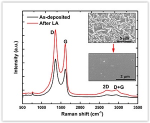
Researchers at North Carolina State University have developed a technique for converting positively charged (p-type) reduced graphene oxide (rGO) into negatively charged (n-type) rGO, creating a layered material that can be used to develop rGO-based transistors for use in electronic devices.
“Graphene is extremely conductive, but is not a semiconductor; graphene oxide has a bandgap like a semiconductor, but does not conduct well at all – so we created rGO,” says Jay Narayan, the John C. Fan Distinguished Chair Professor of Materials Science and Engineering at NC State and corresponding author of a paper describing the work. “But rGO is p-type, and we needed to find a way to make n-type rGO. And now we have it for next-generation, two-dimensional electronic devices.”
Specifically, Narayan and Anagh Bhaumik – a Ph.D. student in his lab – demonstrated two things in this study. First, they were able to integrate rGO onto sapphire and silicon wafers – across the entire wafer.
Second, the researchers used high-powered laser pulses to disrupt chemical groups at regular intervals across the wafer. This disruption moved electrons from one group to another, effectively converting p-type rGO to n-type rGO. The entire process is done at room temperature and pressure using high-power nanosecond laser pulses, and is completed in less than one-fifth of a microsecond. The laser radiation annealing provides a high degree of spatial and depth control for creating the n-type regions needed to create p-n junction-based two-dimensional electronic devices.
The end result is a wafer with a layer of n-type rGO on the surface and a layer of p-type rGO underneath.
This is critical, because the p-n junction, where the two types meet, is what makes the material useful for transistor applications.
Share on:


Suggested Items
Book Excerpt: The Printed Circuit Assembler’s Guide to... Factory Analytics
04/24/2024 | I-Connect007 Editorial TeamIn our fast-changing, deeply competitive, and margin-tight industry, factory analytics can be the key to unlocking untapped improvements to guarantee a thriving business. On top of that, electronics manufacturers are facing a tremendous burden to do more with less. If you don't already have a copy of this book, what follows is an excerpt from the introduction chapter of 'The Printed Circuit Assembler’s Guide to... Factory Analytics: Unlocking Efficiency Through Data Insights' to whet your appetite.
Elevating PCB Design Engineering With IPC Programs
04/24/2024 | Cory Blaylock, IPCIn a monumental stride for the electronics manufacturing industry, IPC has successfully championed the recognition of the PCB Design Engineer as an official occupation by the U.S. Department of Labor (DOL). This pivotal achievement not only underscores the critical role of PCB design engineers within the technology landscape, but also marks the beginning of a transformative journey toward nurturing a robust, skilled workforce ready to propel our industry into the future.
Winner of The Science Show Rakett 69 Receives Incap Scholarship
04/24/2024 | IncapThe winner of the Rakett 69 science show, Andri Türkson, who stood out as an electronics enthusiast, received a scholarship from Incap Estonia, along with an internship opportunity in Saaremaa.
Alternative Manufacturing Inc. Awarded QML Requalification to IPC J-STD-001 and IPC-A-610
04/24/2024 | IPCIPC's Validation Services Program has awarded an IPC J-STD-001 and IPC-A-610 Qualified Manufacturers Listing (QML) requalification to Alternative Manufacturing Inc (AMI).
Boeing's Janene Stinson Earns IPC Excellence in Education Award at IPC APEX EXPO 2024
04/22/2024 | IPCThe IPC Excellence in Education award was presented to Janene Stinson, Boeing, at IPC APEX EXPO 2024 in Anaheim, California, in recognition of her significant contributions to workforce development and leadership.