


 The Right Approach: I Hear the Train A Comin'
 It’s Only Common Sense: OCCAM—the Time Is Now
 Marcy's Musings: The Growing Industry
Tiny Black Holes Enable a New Type of Photodetector for High-Speed Data
April 5, 2017 | UC DavisEstimated reading time: 2 minutes
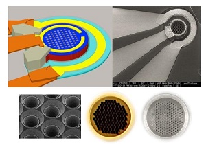
Tiny “black holes” on a silicon wafer make for a new type of photodetector that could move more data at lower cost around the world or across a data center. The technology, developed by electrical engineers at the University of California, Davis, and W&WSens Devices Inc. of Los Altos, California, a Silicon Valley startup, is described in a paper published April 3 in the journal Nature Photonics.
Tapered black holes in silicon, about 1 micrometer in size, can trap photons and act as a photodetector for high-speed data connections. (Saif Islam, UC Davis)
“We’re trying to take advantage of silicon for something silicon cannot usually do,” said Saif Islam, professor of electrical and computer engineering at UC Davis, who co-led the project together with the collaborators at W&WSens Devices Inc. Existing high-speed photodetector devices use materials such as gallium arsenide. “If we don’t need to add nonsilicon components and can monolithically integrate with electronics into a single silicon chip, the receivers become much cheaper.”
The new detector uses tapered holes in a silicon wafer to divert photons sideways, preserving the speed of thin-layer silicon and the efficiency of a thicker layer. So far, Islam’s group has built an experimental photodetector and solar cell using the new technology. The photodetector can convert data from optical to electronics at 20 gigabytes per second (or 25 billion bits per second, more than 200 times faster than your cable modem) with a quantum efficiency of 50 percent, the fastest yet reported for a device of this efficiency.
Data centers need fast connections
The growth of data centers that power the internet “cloud” has created a demand for devices to move large amounts of data, very fast, over short distances of a few yards to hundreds of yards. Such connections could also be used for high-speed home connections, Islam said.
When computer engineers want to move large amounts of data very fast, whether across the world or across a data center, they use fiber-optic cables that transmit data as pulses of light. But these signals need to be converted to electronic pulses at the receiving end by a photodetector. You can use silicon as a photodetector — incoming photons generate a flow of electrons. But there’s a tradeoff between speed and efficiency. To capture most of the photons, the piece of silicon needs to be thick, and that makes it relatively slow. Make the silicon thinner so it works faster, and too many photons get lost.
Instead, circuit designers have used materials such as gallium arsenide and indium phosphide to make high-speed, high-efficiency photodetectors. Gallium arsenide, for example, is about 10 times as efficient as a silicon at the same scale and wavelength. But it is significantly more expensive and cannot be monolithically integrated with silicon electronics.
Tapered holes as light traps
Islam’s group began by experimenting with ways to increase the efficiency of silicon by adding tiny pillars or columns, then holes to the silicon wafer. After two years of experiments, they settled on a pattern of holes that taper toward the bottom.“We came up with a technology that bends the incoming light laterally through thin silicon,” Islam said.The idea is that photons enter the holes and get pulled sideways into the silicon. The wafer itself is about 2 microns thick, but because they move sideways, the photons travel through 30 to 40 microns of silicon, like the ripple of waves on a pond when a pebble is dropped into the water.
The holes-based device can also potentially work with a wider range of wavelengths of light than current technology, Islam said.
Share on:


Suggested Items
Warm Windows and Streamlined Skin Patches – IDTechEx Explores Flexible and Printed Electronics
04/26/2024 | IDTechExFlexible and printed electronics can be integrated into cars and homes to create modern aesthetics that are beneficial and easy to use. From luminous car controls to food labels that communicate the quality of food, the uses of this technology are endless and can upgrade many areas of everyday life.
iNEMI Packaging Tech Topic Series: Role of EDA in Advanced Semiconductor Packaging
04/26/2024 | iNEMIAdvanced semiconductor packaging with heterogenous integration has made on-package integration of multiple chips a crucial part of finding alternatives to transistor scaling. Historically, EDA tools for front-end and back-end design have evolved separately; however, design complexity and the increased number of die-to-die or die-to-substrate interconnections has led to the need for EDA tools that can support integration of overall design planning, implementation, and system analysis in a single cockpit.
Koh Young Showcases Award-winning Inspection Solutions at SMTconnect with SmartRep in Hall 4A.225
04/25/2024 | Koh Young TechnologyKoh Young Technology, the industry leader in True 3D measurement-based inspection solutions, will showcase an array of award-winning inspection and measurement solutions at SMTconnect alongside its sales partner, SmartRep, in booth 4A.225 at NürnbergMesse from June 11-13, 2023. The following offers a glimpse into what Koh Young will present at the tradeshow:
Real Time with… IPC APEX EXPO 2024: Plasmatreat: Innovative Surface Preparation Solutions
04/25/2024 | Real Time with...IPC APEX EXPOIn this interview, Editor Nolan Johnson speaks with Hardev Grewal, CEO and president of Plasmatreat, a developer of atmospheric plasma solutions. Plasmatreat uses clean compressed air and electricity to create plasma, offering environmentally friendly methods for surface preparation. Their technology measures plasma density for process optimization and can remove organic micro-contamination. Nolan and Hardev also discuss REDOX-Tool, a new technology for removing metal oxides.
Nanotechnology Market to Surpass $53.51 Billion by 2031
04/25/2024 | PRNewswireSkyQuest projects that the nanotechnology market will attain a value of USD 53.51 billion by 2031, with a CAGR of 36.4% over the forecast period (2024-2031).