


 It’s Only Common Sense: OCCAM—the Time Is Now
 Marcy's Musings: The Growing Industry
 Dan’s Biz Bookshelf: Seeing the How
Graphene - A Wonder Material for Electronic Devices
May 3, 2017 | DTU NanotechEstimated reading time: 3 minutes
In collaboration with partners from industry and academia, researchers at DTU Nanotech have improved the possibility of utilizing the extraordinary properties of graphene for energy efficient optoelectronic devices.
The two dimensional material graphene has attracted great attention since it was first isolated and characterized in 2004. PhD Student Patrick Whelan explains: “There is definitely something to be excited about with the list of extraordinary properties that comes with graphene; it is the mechanically strongest compound discovered, it has a high transparency, it is an efficient conductor of heat and electricity, it is flexible and foldable and the list goes on”.
Graphene has been predicted to play a major role in the electronics industry especially as a transparent conducting electrode for organic light emitting diodes (OLEDs), solar cells and wearable electronics.
Transfer of graphene is the bottleneck
Fabrication of large areas of graphene by chemical vapor deposition onto copper catalysts is reaching industrial maturity. In order to integrate graphene into a device it must be transferred from the catalyst onto a suitable target substrate such as glass without introducing any defects in the graphene layer. Patrick Whelan says that “the main focus of my PhD project has been to develop new transfer techniques. We would like to develop methods that do not damage the graphene layer and which are non-destructive towards the copper substrate.”
At DTU Nanotech, a method for accurately monitoring the decoupling of graphene from copper catalysts during oxidation in water has been developed. The method is based on the so-called Raman spectroscopy, a standard characterization tool in the graphene community. Patrick Whelan explains that “using the new method, it is possible for us to measure if the graphene is fully decoupled from the copper catalysts and thus we have been able to transfer graphene by mechanical peeling from 12inch diameter copper thin films”. (See figure 1).
Figure 1: Transferring graphene from a 12 inch copper substrate using a supporting polymer film
Patrick’s research is part of two larger research projects involving a number of industrial as well as academic partners. One of these partners is Cambridge University where Patrick had an external stay. The collaboration in Cambridge resulted in the development of another new transfer method, where the graphene is released from the copper substrate by intercalation of basic solution between graphene and copper. The electrical properties of graphene transferred by this method are superior when compared to standard transfer techniques.
Graphene-based OLEDs
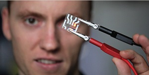
The new transfer technique developed at Cambridge University has made it possible to fabricate OLEDs where graphene is used as replacement for indium tin oxide (ITO) as transparent conducting electrode (see figure 2). These OLEDs are made in collaboration with Fraunhofer COMEDD (Dresden, Germany) which is a research project partner specialized in organic electronics. Today, ITO is the material which is most frequently used as transparent conducting electrode. However, the researchers are able to achieve higher power efficiencies from OLEDs built on a single layer of graphene compared to ITO-based OLEDs.
Figure 2: OLED with graphene as transparent top electrode
Patrick explains that “the next step is to focus on increasing the conductivity of the transferred graphene layers and thus the power efficiency of the OLEDs. We see two possible routes for this: We can stack multiple graphene layers and/or we can dope the graphene chemically, that is we can introduce impurities that affect the electrical properties. This should enable graphene to be even more competitive with ITO”.
At DTU Fotonik the conductivity of the graphene can be mapped by the so-called THz spectroscopy, a fast and non-contact measuring technique, which makes it easy to test the influence of different doping methods.
“In the future, we hope that graphene can become the standard material as electrode for flexible electronics, which for instance can be used to make bendable screens. The markets for wearable electronics and e-textiles are expected to grow over the coming years and it is possible that graphene could also play a role in such products due to its flexibility, conductivity, and light weight”, says Patrick.
The research was carried out in the DA-GATE (Danish Alliance for Graphene Applications, Technology and Engineering) project, funded by Innovation Fund Denmark, and the GLADIATOR (Graphene Layers: Production, Characterization and Integration) project funded by EU FP7.
Share on:


Suggested Items
Insulectro’s 'Storekeepers' Extend Their Welcome to Technology Village at IPC APEX EXPO
04/03/2024 | InsulectroInsulectro, the largest distributor of materials for use in the manufacture of PCBs and printed electronics, welcomes attendees to its TECHNOLOGY VILLAGE during this year’s IPC APEX EXPO at the Anaheim Convention Center, April 9-11, 2024.
ENNOVI Introduces a New Flexible Circuit Production Process for Low Voltage Connectivity in EV Battery Cell Contacting Systems
04/03/2024 | PRNewswireENNOVI, a mobility electrification solutions partner, introduces a more advanced and sustainable way of producing flexible circuits for low voltage signals in electric vehicle (EV) battery cell contacting systems.
Heavy Copper PCBs: Bridging the Gap Between Design and Fabrication, Part 1
04/01/2024 | Yash Sutariya, Saturn Electronics ServicesThey call me Sparky. This is due to my talent for getting shocked by a variety of voltages and because I cannot seem to keep my hands out of power control cabinets. While I do not have the time to throw the knife switch to the off position, that doesn’t stop me from sticking screwdrivers into the fuse boxes. In all honesty, I’m lucky to be alive. Fortunately, I also have a talent for building high-voltage heavy copper circuit boards. Since this is where I spend most of my time, I can guide you through some potential design for manufacturability (DFM) hazards you may encounter with heavy copper design.
Trouble in Your Tank: Supporting IC Substrates and Advanced Packaging, Part 5
03/19/2024 | Michael Carano -- Column: Trouble in Your TankDirect metallization systems based on conductive graphite or carbon dispersion are quickly gaining acceptance worldwide. Indeed, the environmental and productivity gains one can achieve with these processes are outstanding. In today’s highly competitive and litigious environment, direct metallization reduces costs associated with compliance, waste treatment, and legal issues related to chemical exposure. What makes these processes leaders in the direct metallization space?
AT&S Shines with Purest Copper on World Recycling Day
03/18/2024 | AT&SThe Styrian microelectronics specialist AT&S is taking World Recycling Day as an opportunity to review the progress that has been made in recent months at its sites around the world in terms of the efficient use of resources: