


 The Right Approach: I Hear the Train A Comin'
 It’s Only Common Sense: OCCAM—the Time Is Now
 Marcy's Musings: The Growing Industry
'Persistent Photoconductivity' Offers New Tool for Bioelectronics
May 3, 2017 | NC State UniversityEstimated reading time: 1 minute
Researchers at North Carolina State University have developed a new approach for manipulating the behavior of cells on semiconductor materials, using light to alter the conductivity of the material itself.
“There’s a great deal of interest in being able to control cell behavior in relation to semiconductors – that’s the underlying idea behind bioelectronics,” says Albena Ivanisevic, a professor of materials science and engineering at NC State and corresponding author of a paper on the work. “Our work here effectively adds another tool to the toolbox for the development of new bioelectronic devices.”
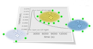
The new approach makes use of a phenomenon called persistent photoconductivity. Materials that exhibit persistent photoconductivity become much more conductive when you shine a light on them. When the light is removed, it takes the material a long time to return to its original conductivity.
When conductivity is elevated, the charge at the surface of the material increases. And that increased surface charge can be used to direct cells to adhere to the surface.
“This is only one way to control the adhesion of cells to the surface of a material,” Ivanisevic says. “But it can be used in conjunction with others, such as engineering the roughness of the material’s surface or chemically modifying the material.”
For this study, the researchers demonstrated that all three characteristics can be used together, working with a gallium nitride substrate and PC12 cells – a line of model cells used widely in bioelectronics testing.
The researchers tested two groups of gallium nitride substrates that were identical, except that one group was exposed to UV light – triggering its persistent photoconductivity properties – while the second group was not.
“There was a clear, quantitative difference between the two groups – more cells adhered to the materials that had been exposed to light,” Ivanisevic says.
“This is a proof-of-concept paper,” Ivanisevic says. “We now need to explore how to engineer the topography and thickness of the semiconductor material in order to influence the persistent photoconductivity and roughness of the material. Ultimately, we want to provide better control of cell adhesion and behavior.”
Share on:


Suggested Items
SMC Korea 2024 to Highlight Semiconductor Materials Trends and Innovations on Industry’s Path to $1 Trillion
04/24/2024 | SEMIWith Korea a major consumer of semiconductor materials and advanced materials a key driver of innovation on the industry’s path to $1 trillion, industry leaders and experts will gather at SMC (Strategic Materials Conference) Korea 2024 on May 29 at the Suwon Convention Center in Gyeonggi-do, South Korea to provide insights into the latest materials developments and trends. Registration is open.
Groundbreaking Ceremony Marks the Beginning of a New Era for Newccess Industrial; The Construction of the MINGXIN Building
04/12/2024 | Newccess IndustrialOn a clear and sunny day in March, the groundbreaking ceremony for the MINGXIN Building took place in Shenzhen, China. This moment marked the official commencement of construction for a project that will reshape the semiconductor materials industry.
The Need for a Holistic Global Sustainability Standard
04/10/2024 | Michael Ford, Aegis SoftwareNo one can deny that the resources of our fragile planet are finite. The environment seems like a third party, subject to constant degradation. We’re acutely aware of the effects of pollution on our climate, and despite our “throw-away” culture, recycling and recovery of materials has remained relatively expensive, even as we use more energy just to survive.
iNEMI Publishes Four Roadmap Topics
04/04/2024 | iNEMIThe International Electronics Manufacturing Initiative (iNEMI) announces the availability of the first roadmap topics in the new iNEMI Roadmap format. Printed circuit boards, sustainable electronics, smart manufacturing, and mmWave materials and test are now available online.
Insulectro’s 'Storekeepers' Extend Their Welcome to Technology Village at IPC APEX EXPO
04/03/2024 | InsulectroInsulectro, the largest distributor of materials for use in the manufacture of PCBs and printed electronics, welcomes attendees to its TECHNOLOGY VILLAGE during this year’s IPC APEX EXPO at the Anaheim Convention Center, April 9-11, 2024.