


 The Right Approach: I Hear the Train A Comin'
 It’s Only Common Sense: OCCAM—the Time Is Now
 Marcy's Musings: The Growing Industry
Evidence of Topological Excitations in a Quantum Magnet
May 15, 2017 | London Centre for NanotechnologyEstimated reading time: 3 minutes
Condensed matter physics is the study of the multitude of ways that matter can organise itself. In each phase as conventionally understood, be it a magnet, metal, superconductor or something else, it is possible to characterise the phase by looking at the system locally in space.
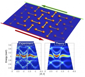
Figure Caption: The top panel shows the orthogonal arrangement of “dimers” in SCBO. The dimers are formed of pairs of magnetic copper ions which are in a quantum mechanical superposition with zero total magnetic moment. It requires a finite energy to break-up this superposition and induce a net moment. These excitations are called “triplons”, in order to express that they behave as quantum mechanical particles. The coupling between spins of adjacent dimers is responsible for the peculiar motion of triplons as well as for the strong interactions between them. In a small magnetic field perpendicular to the dimer planes, the magnetic excitation acquire a topological character. This goes hand-in-hand with the appearance of excitations that circulate around the edges of the sample. The bottom panel shows the comparison between the excitations measured by inelastic neutron scattering using the LET spectrometer at ISIS and theoretical calculations based on a model of interacting triplons. Because of the high resolution and sensitivity of the LET spectrometer it was possible to measure the magnetic excitations of SCBO in unprecedented detail and to observe fingerprints of strong interactions.
Over the last ten years, there has been a revolution in our understanding of matter through the realisation that there are states of matter that cannot be distinguished with local observations alone. Instead one must, in some sense, know something about the system as a whole. The distinction between such phases is encoded in so-called topological numbers which are precise measures of the nature of these phases. To take an analogy, we might ask how you could tell that the Earth is roughly spherical rather than being punctured by holes like a pretzel. By standing at any point on the Earth you would not be able to tell. Instead you need a global observation. For example, you may notice that the shadow during a lunar eclipse does not have holes. In this case, the topology is reflected in the number of holes. In so-called topological insulators, the topological number is computed from the quantum mechanical wave function of the electrons.
Such topological phases have experimental signatures even though we cannot distinguish them locally from more conventional phases. This is because, when there is a boundary between a topological insulator and a trivial insulator, the boundary conducts electricity like a metal - the presence of this surface state being determined by the topology of the solid.
In this new Nature Physics paper from a team of theorists and experimentalists at the LCN, Oxford and the Rutherford-Appleton Laboratory, our understanding of condensed matter systems is advanced by showing that such topological states can arise in a completely new setting. The paper presents experimental evidence that in a particular quantum magnet SrCu2(BO3)2 (SCBO) topology plays an important role.
As depicted in the figure, the material has magnetic copper ions sitting on a lattice such that the magnetic interactions bind the magnetic moments together into pairs of total spin zero. One implication of the reported experiment is that, in contrast to usual topological insulators which have metallic surface states, SCBO instead has topological surface states which are entirely magnetic. In fact, unlike the usual topological insulators, the surface states exist in the excited states above the lowest energy spin zero ground state and they carry magnetic currents in a particular direction around the edge of the system.
In short, these findings are an important breakthrough because it paves the way to the exploration of a completely new set of topological insulating materials with novel properties. The form the basis of further potential research to understand the extent to which such systems occur in nature and how their unusual properties may be used in future technologies - perhaps using their unusual magnetic currents to store and transmit information.
Share on:


Suggested Items
Designer’s Notebook: What Designers Need to Know About Manufacturing, Part 2
04/24/2024 | Vern Solberg -- Column: Designer's NotebookThe printed circuit board (PCB) is the primary base element for providing the interconnect platform for mounting and electrically joining electronic components. When assessing PCB design complexity, first consider the component area and board area ratio. If the surface area for the component interface is restricted, it may justify adopting multilayer or multilayer sequential buildup (SBU) PCB fabrication to enable a more efficient sub-surface circuit interconnect.
Insulectro’s 'Storekeepers' Extend Their Welcome to Technology Village at IPC APEX EXPO
04/03/2024 | InsulectroInsulectro, the largest distributor of materials for use in the manufacture of PCBs and printed electronics, welcomes attendees to its TECHNOLOGY VILLAGE during this year’s IPC APEX EXPO at the Anaheim Convention Center, April 9-11, 2024.
ENNOVI Introduces a New Flexible Circuit Production Process for Low Voltage Connectivity in EV Battery Cell Contacting Systems
04/03/2024 | PRNewswireENNOVI, a mobility electrification solutions partner, introduces a more advanced and sustainable way of producing flexible circuits for low voltage signals in electric vehicle (EV) battery cell contacting systems.
Heavy Copper PCBs: Bridging the Gap Between Design and Fabrication, Part 1
04/01/2024 | Yash Sutariya, Saturn Electronics ServicesThey call me Sparky. This is due to my talent for getting shocked by a variety of voltages and because I cannot seem to keep my hands out of power control cabinets. While I do not have the time to throw the knife switch to the off position, that doesn’t stop me from sticking screwdrivers into the fuse boxes. In all honesty, I’m lucky to be alive. Fortunately, I also have a talent for building high-voltage heavy copper circuit boards. Since this is where I spend most of my time, I can guide you through some potential design for manufacturability (DFM) hazards you may encounter with heavy copper design.
Trouble in Your Tank: Supporting IC Substrates and Advanced Packaging, Part 5
03/19/2024 | Michael Carano -- Column: Trouble in Your TankDirect metallization systems based on conductive graphite or carbon dispersion are quickly gaining acceptance worldwide. Indeed, the environmental and productivity gains one can achieve with these processes are outstanding. In today’s highly competitive and litigious environment, direct metallization reduces costs associated with compliance, waste treatment, and legal issues related to chemical exposure. What makes these processes leaders in the direct metallization space?