


 The Right Approach: I Hear the Train A Comin'
 It’s Only Common Sense: OCCAM—the Time Is Now
 Marcy's Musings: The Growing Industry
Photonic 'Hypercrystals' Shed Stronger Light
May 31, 2017 | Purdue UniversityEstimated reading time: 3 minutes
Sources that integrate two artificial optical material concepts may drive ultrafast “Li-Fi” communications.
In many applications, Li-Fi through-the-air optical networks potentially offer major advantages over Wi-Fi and other radiofrequency systems. Li-Fi nets can operate at extremely high speeds. They can exploit an extremely broad spectrum of frequencies. They avoid the interference problems that plague radiofrequency systems, which are especially problematic in high-security environments such as airplane cockpits and nuclear power stations. They are less open to hackers. And while their range is relatively limited, they don’t need line-of-sight connections to operate, said Evgenii Narimanov, a Purdue University professor of electrical and computer engineering.
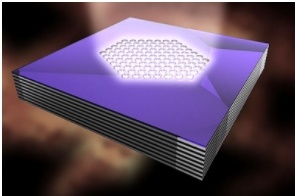
This drawing depicts a “photonic hypercrystal,” which is promising for future “Li-Fi” technologies that offer major advantages over Wi-Fi and other radiofrequency communications systems. (Image courtesy of Tal Galfsky, CCNY)
Today’s Li-Fi nets can’t fully achieve all these potential benefits because they lack suitable light sources, he said.
But designs that integrate two optical material concepts into “photonic hypercrystals” may fill this gap.
Narimanov first proposed this concept in 2014. This month, he and colleagues at the City College of New York reported demonstrations of photonic hypercrystals with greatly increased light emission rates and intensities in the Proceedings of the National Academy of Sciences (PNAS).
Photonic hypercrystals combine the properties of metamaterials and photonic crystals, both “artificial” optical materials with properties that are not usually found in nature, Narimanov said.
Metamaterials are created from artificial building blocks that are much smaller than the wavelength of light, while in photonic crystals the size of the “unit cell” is comparable to this wavelength. While these two types of composite materials generally show very different properties, the photonic hypercrystals combine them all within the same structure.
Photonic hypercrystals are based on one type called hyperbolic metamaterials, which can be built with alternating layers of metal and dielectric materials—where the electrical current can only travel along the metallic layers.
“Generally, for light, metals and dielectrics are fundamentally different: light can travel in dielectrics, but is reflected back from metals,” Narimanov said. "But a hyperbolic metamaterial behaves as metal along the layers and as a dielectric in the direction perpendicular to the layers, at the same time. For light, hyperbolic media is, therefore, the third estate of matter, entirely different from the usual metals and dielectrics.”
Among the interesting properties that this structure produces, the metamaterial accommodates a large number of photonic states, allowing spontaneous light emission at extremely high rates.
“For a light source, the problem is that this light in the hyperbolic metamaterial can’t get out,” said Narimanov.
Enter photonic crystals—periodic nanostructures that can manipulate optical interference to optimize light transmission.
In the integrated photonic hypercrystals presented in the PNAS paper, the hyperbolic metamaterial consists of alternating layers of silver (the metal) and aluminum oxide (the dielectric). Hexagonal arrays of holes milled into the layers create the photonic crystal. In the design, the visible light is emitted by quantum dots (semiconductor nanoparticles that can emit light) embedded in one of the layers that form the hyperbolic metamaterial.
The result: extremely high levels of control and enhancement of the emitted light.
“These photonic hypercrystals were fabricated at the City University of New York’s Advanced Science Research Center using standard nano- and micro-fabrication techniques such as thin film evaporation and focused ion beam milling,” said Tal Galfsky, a CCNY graduate student who is lead author on the PNAS paper. “These techniques are scalable with modern industry capabilities. "
Vinod Menon, CCNY professor of physics, is senior author on the paper, and CCNY graduate student Jie Gu also contributed to the work.
The work reported in PNAS demonstrates that “on a fundamental level, the problem of designing photonic hypercrystals has been solved,” said Narimanov.
He cautions, however, that significant engineering challenges must be overcome before these devices can be commercialized. Among these barriers, the demonstration devices are pumped optically by a laser, but commercial versions will need to be driven electrically and incorporate either semiconductor or organic LEDs, he said.
As they mature, photonic hypercrystals also may fill many other demanding roles in ultrafast optoelectronics. One of the most promising avenues of research, Narimanov suggested, is to create more efficient versions of the single-photon guns employed in quantum information processing.
The research was supported by the Army Research Office, the National Science Foundation and the Gordon and Betty Moore Foundation.
Writer: Eric Bender
Source: Evgenii Narimanov, 765-494-1622, evgenii@purdue.edu
Share on:


Suggested Items
Growth Potential: Electronics Manufacturing Driving Massive Surge in Manufacturing Investment
04/22/2024 | Shawn DuBravac, IPCIn the early months of the pandemic, investment in manufacturing infrastructure, such as plants and production facilities, declined sharply. Real investment dropped over 11%, before finally recovering to pre-pandemic levels in the first half of 2022. Over the past two years, however, several factors have combined to drive manufacturing investment to record levels.
Digitalisation and ESG
04/19/2024 | Marina Hornasek-Metzl, AT&SDigitalisation and ESG are prominent and high-priority topics in the global business community. The first focuses on applying technology throughout the value chain to produce faster, smarter, and more desirable business outcomes. The latter emphasises the broader value a business is expected to create for its stakeholders from an environmental, social, and governance perspective.
Designing Electronics for High Thermal Loads
04/16/2024 | Akber Roy, Rush PCB Inc.Developing proactive thermal management strategies is important in the early stages of the PCB design cycle to minimize costly redesign iterations. Here, I delve into key aspects of electronic design that hold particular relevance for managing heat in electronic systems. Each of these considerations plays a pivotal role in enhancing the reliability and performance of the overall system.
FPT Unveils Strategic Directions, “All In” on AI, Automotive and Semiconductor
04/15/2024 | BUSINESS WIREFPT Corporation (FPT) announced its strategic directions for the 2024-2026 period at the 2024 Annual General Meeting, with five focused areas defined as Artificial Intelligence (AI), Automotive, Semiconductor, Digital Transformation, and Green Transformation.
It’s Only Common Sense: Here’s What To Do After IPC APEX EXPO 2024
04/15/2024 | Dan Beaulieu -- Column: It's Only Common SenseYou had a great time last week at IPC APEX EXPO 2024. Now you’re back home and ready to go on to other things. Au contraire mon frère. Now the work really gets started, and you must capitalize on all the good work you did last week. Follow up on the connections you made, the leads you created, and the partnerships and relationships you developed.