


 It’s Only Common Sense: OCCAM—the Time Is Now
 Marcy's Musings: The Growing Industry
 Dan’s Biz Bookshelf: Seeing the How
Where is the Semiconductor Manufacturing Sweet Spot?
June 1, 2017 | Semico ResearchEstimated reading time: 1 minute
Where is the semiconductor manufacturing sweet spot? Two recent Semico Research Corp. studies provide the information to not only determine the overall sweet spot but to dig even further to find which products and technologies are the driving forces behind the growth or decline.
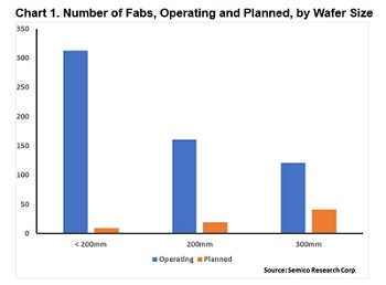
Chart 1. Number of Fabs, Operating and Planned, by Wafer Size
Chart 1, was developed from data in the fab database study. It shows the number of fabs operating and planned by wafer size.
Surprisingly, there are still more than 350 fabs operating at 150mm or smaller. Many manufacture trailing edge devices, especially discretes, while others manufacture relatively new devices, including analog, power, MEMS and LED devices. These semiconductors are not leading-edge devices, but they are essential to many electronics industry end-use products. The die size for many is quite small, and they do not scale well to smaller geometries. Many may continue to be manufactured in 150mm fabs for the immediate future. Others will undoubtedly migrate to 200mm fabs.
There were more than 150 fabs manufacturing devices on 200mm wafers in 2016. Many are producing MOS Logic semiconductors, but there is a sprinkling of 200mm fabs producing a wide variety of other semiconductor product types including analog semiconductors, MEMS devices, power semiconductors, and SRAM. Nineteen new 200mm fabs are planned or under construction.
There were more than 100 fabs operating at 300mm in 2016. These fabs are focused on high-volume devices manufactured at leading-edge technology nodes, including MPUs, DRAM, and NAND Flash. Following the usual pattern, many semiconductor product types will migrate from 200mm to 300mm fabs. More than 40 additional 300mm fabs are planned or under construction.
Chart 2. Wafer Demand by Technology Node
Chart 2, below, developed from data in the wafer demand study, shows wafer demand by technology node.
The first category, greater than or equal to 800nm, was chosen because it represents most manufacturing in 150mm or smaller fabs. The second category, 500nm through 130nm, was chosen because it represents most manufacturing in 200mm fabs. The CAGR for 2016 through 2021 for this category is 4.6%. Most 300mm fabs are at technology nodes beyond 100nm, the third category. The CAGR for 2016 through 2021 for this category is 9.8%.
So, where is the semiconductor manufacturing sweet spot? It depends. The sweet spot for new fabs is 300mm, with 200mm fabs close behind. The sweet spot for wafer demand is 300mm wafers.
Share on:


Suggested Items
Elevating PCB Design Engineering With IPC Programs
04/24/2024 | Cory Blaylock, IPCIn a monumental stride for the electronics manufacturing industry, IPC has successfully championed the recognition of the PCB Design Engineer as an official occupation by the U.S. Department of Labor (DOL). This pivotal achievement not only underscores the critical role of PCB design engineers within the technology landscape, but also marks the beginning of a transformative journey toward nurturing a robust, skilled workforce ready to propel our industry into the future.
Fujitsu, METRON Collaborate to Drive ESG Success
04/24/2024 | JCN NewswireFujitsu Limited and METRON SAS, a French cleantech company specializing in energy management solutions for industrial decarbonization, today announced a strategic initiative to contribute to the realization of carbon neutrality in the manufacturing industry.
Real Time with... IPC APEX EXPO 2024: Final Finishes and IC Substrate Manufacturing
04/24/2024 | Real Time with...IPC APEX EXPOEditor Marcy LaRont and Richard DePoto, Uyemura's Business Development Manager, engage in a comprehensive discussion about the positive aspects of the show, the benefits of RAIG in final finishes, and the hurdles faced when upgrading your surface finish. Also discussed are the role of Uyemura's MEC pretreatment agents in IC substrate manufacturing and the importance of collaboration and knowledge sharing.
Women MAKE Awards Recognizes GlobalFoundries’ Jennifer Robbins and Katelyn Harrison for Manufacturing Excellence
04/24/2024 | GlobalFoundriesThe Manufacturing Institute (MI)—the workforce development and education affiliate of the National Association of Manufacturers—honored two outstanding women from GlobalFoundries (GF) at their annual Women MAKE Awards. Jennifer (Jenny) Robbins, Senior Director, Central Facilities, was recognized as a 2024 Women MAKE Awards Honoree, while Katelyn Harrison, Senior Integration Engineer, was honored as an Emerging Leader.
GlobalFoundries Commits to Achieving Net Zero Emissions and Carbon-Neutral Power by 2050
04/23/2024 | GlobalFoundriesGlobalFoundries (GF) is furthering its commitment to sustainable operations and fighting climate change with the announcement of two new long-term goals to achieve net-zero greenhouse gas (GHG) emissions and 100% carbon-neutral power by 2050.