


 It’s Only Common Sense: OCCAM—the Time Is Now
 Marcy's Musings: The Growing Industry
 Dan’s Biz Bookshelf: Seeing the How
Component Tracking Solution via 'Fingerprint'
June 5, 2017 | Fraunhofer-GesellschaftEstimated reading time: 3 minutes
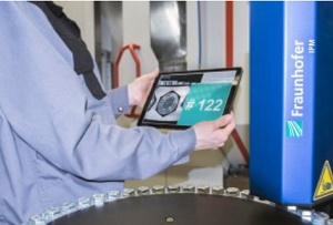
Highly interconnected manufacturing chains, cost issues and technical feasibility make it difficult to trace individual components in mass production. Efficient “track & trace“ solutions are, however, an important prerequisite for production and process optimization — especially in the context of digitized manufacturing. With its “Track & Trace Fingerprint“ solution, the Fraunhofer-Institute for Physical Measurement Techniques IPM in Freiburg, Germany, has developed a marker-free system for tracing mass components.
With its “Track & Trace Fingerprint“ Fraunhofer IPM has developed a marker-free system for the traceability of mass components.
In times of highly networked production processes and global supply chains, it is a challenge for the industry to trace individual components of complex products in retrospect. RFID tags, DataMatrix codes and even chemical markers are being used for the identification of high-priced components. However, for reasons of practicality, the complete traceablity of components and production histories in mass production is also necessary, because even the smallest and — what may at first glance appear to be —most insignificant parts can compromise the quality of a complex and expensive end product. “Therefore, practical and at the same time inexpensive ‘track & trace‘ solutions are required for small, price-sensitive items, such as electrical connectors or spark plugs. Labels or special markers often prove to be too expensive or technically impracticable,“ explains Dr. Alexander Förste, project manager of “Track & Trace Fingerprint“ at the Fraunhofer IPM. “In order to tackle this problem, we have developed an efficient traceability system for mass components using ‘Track & Trace Fingerprint‘, which enables the individual recognition and authentication of individual components.“
Mass components are also unique
The new Fraunhofer technology uses the individual surface micro-structure and color texture of components and semi-finished products. First, a selected area of the component with all its specific structures and position is recorded with a high-resolution industrial camera. A characteristic bit sequence — the fingerprint — is computed from the resulting image and assigned to an individual ID. This pairing is then stored in a database. The ID can then be linked with further information such as measurement or production data. In order to identify a component later on, the process is simply repeated — a reconciliation process of the data after the image was recorded reliably and exactly provides the corresponding fingerprint code and thus further individual features of the component.
“It is forbidden to engrave a serial number or barcode on the sealing surface as well as on the decorative surface. Our new approach, on the other hand, is efficient, practical and cost-saving where mass components are concerned: a wide range of materials is suitable for this type of marker-free traceability — from smooth plastics to aluminum and from cast iron to painted surfaces,“ explains Förste. “Every second, the device can unambiguously identify the stochastic ‘fingerprint‘ of a component even in batch sizes of several 100,000 pieces; this allows an allocation of component-related data in the production cycle. Since no additional markers or IDs are attached to the product, this system is not only tamper-proof but also very economically feasible. Ultimately, no additional quantity-related costs are incurred.“ Due to the large number of possible measuring points, the robust object recognition works reliably even in case of interfering influences such as contamination or scratches.
No process optimization without traceability
Complete and marker-free traceability over the entire manufacturing process creates a tangible added value, especially in industries with high quality standards such as the automotive industry or medical technology. Fraunhofer IPM has already deployed a first prototype of the new process in the “Track4Quality“ project. Moreover, a pilot installation will be put into operation with a partner from the automotive supply industry during the second half of 2017. “Our technology clearly demonstrates how the networking of digitization and measuring technology in conventional production processes works in practice against the backdrop of the fourth industrial revolution,“ says Förste. The quality of complex industrial products can depend on the quality of each individual component. If only one single faulty connector costing just a few cents endangers the functionality and longevity of a complex electronic control box of, for example, a car, then all installed connectors are considered to be a liability. Our procedure prevents such costly and cost-intensive operations in the production and value chain.“ If manufacturing companies are able to trace even the smallest key components quickly and unequivocally in mass production, they will be able to benefit from decisive process optimization — for example, in the improvement of production and assembly processes, in the case of necessary product recalls or for recycling.
Share on:


Suggested Items
Cadence, TSMC Collaborate on Wide-Ranging Innovations to Transform System and Semiconductor Design
04/25/2024 | Cadence Design SystemsCadence Design Systems, Inc. and TSMC have extended their longstanding collaboration by announcing a broad range of innovative technology advancements to accelerate design, including developments ranging from 3D-IC and advanced process nodes to design IP and photonics.
Designer’s Notebook: What Designers Need to Know About Manufacturing, Part 2
04/24/2024 | Vern Solberg -- Column: Designer's NotebookThe printed circuit board (PCB) is the primary base element for providing the interconnect platform for mounting and electrically joining electronic components. When assessing PCB design complexity, first consider the component area and board area ratio. If the surface area for the component interface is restricted, it may justify adopting multilayer or multilayer sequential buildup (SBU) PCB fabrication to enable a more efficient sub-surface circuit interconnect.
Real Time with... IPC APEX EXPO 2024: Advancements in Laser Depaneling with LPKF
04/24/2024 | Real Time with...IPC APEX EXPOJake Benz, LPKF sales manager for North America, discusses the company's advancements in laser depaneling. LPKF has introduced a green wavelength laser for processing rigid FR-4 circuit boards, bringing significant gains in processing speeds to market. The company transitioned from IR CO2 to UV wavelength due to heat and burning issues.
KYZEN to Focus on AQUANOX A4618 at SMTA Wisconsin Expo & Tech Forum
04/22/2024 | KYZEN'KYZEN, the global leader in innovative environmentally friendly cleaning chemistries, will exhibit at the SMTA Wisconsin Expo & Tech Forum, scheduled to take place Tuesday, May 7, 2024 at the Four Poins by Sheraton, Milwaukee Airport in Milwaukee, WI.
AIM Solder’s Dillon Zhu to Present on Ultraminiature Soldering at SMTA China East
04/22/2024 | AIMAIM Solder, a leading global manufacturer of solder assembly materials for the electronics industry, is pleased to announce that Dillon Zhu will present on the topic: Ultraminiature Soldering: Techniques, Technologies, and Standards at SMTA China East. This event is being held at the Shanghai World Expo Exhibition & Convention Center from April 24-25.