


 Marcy's Musings: The Growing Industry
 It’s Only Common Sense: Here’s What To Do After IPC APEX EXPO 2024
 Dan’s Biz Bookshelf: Seeing the How
Researchers Image Quasiparticles That Could Lead to Faster Circuits, Higher Bandwidths
June 12, 2017 | Iowa State UniversityEstimated reading time: 2 minutes
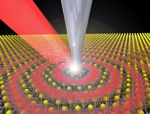
Zhe Fei pointed to the bright and dark vertical lines running across his computer screen. This nano-image, he explained, shows the waves associated with a half-light, half-matter quasiparticle moving inside a semiconductor.
“These are waves just like water waves,” said Fei, an Iowa State University assistant professor of physics and astronomy and an associate of the U.S. Department of Energy’s Ames Laboratory. “It’s like dropping a rock on the surface of water and seeing waves. But these waves are exciton-polaritons.”
Exciton-polaritons are a combination of light and matter. Like all quasiparticles, they’re created within a solid and have physical properties such as energy and momentum. In this study, they were launched by shining a laser on the sharp tip of a nano-imaging system aimed at a thin flake of molybdenum diselenide (MoSe2), a layered semiconductor that supports excitons.
Excitons can form when light is absorbed by a semiconductor. When excitons couple strongly with photons, they create exciton-polaritons.
It’s the first time researchers have made real-space images of exciton-polaritons. Fei said past research projects have used spectroscopic studies to record exciton-polaritons as resonance peaks or dips in optical spectra. Until recent years, most studies have only observed the quasiparticles at extremely cold temperatures – down to about -450 degrees Fahrenheit.
But Fei and his research group worked at room temperature with the scanning near-field optical microscope in his campus lab to take nano-optical images of the quasiparticles.
“We are the first to show a picture of these quasiparticles and how they propagate, interfere and emit,” Fei said.
The researchers, for example, measured a propagation length of more than 12 microns – 12 millionths of a meter – for the exciton-polaritons at room temperature.
Fei said the creation of exciton-polaritons at room temperature and their propagation characteristics are significant for developing future applications for the quasiparticles. One day they could even be used to build nanophotonic circuits to replace electronic circuits for nanoscale energy or information transfer.
Fei said nanophotonic circuits with their large bandwidth could be up to 1 million times faster than current electrical circuits.
A research team led by Fei recently reported its findings in the scientific journal Nature Photonics. The paper’s first author is Fengrui Hu, an Iowa State postdoctoral research associate in physics and astronomy. Additional co-authors are Yilong Luan, an Iowa State doctoral student in physics and astronomy; Marie Scott, a recently graduated undergraduate at the University of Washington; Jiaqiang Yan and David Mandrus of Oak Ridge National Laboratory and the University of Tennessee; and Xiaodong Xu of the University of Washington.
The researchers’ work was supported by funds from Iowa State and the Ames Laboratory to launch Fei’s research program. The W.M. Keck Foundation of Los Angeles also partially supported the nano-optical imaging for the project.
The researchers also learned that by changing the thickness of the MoSe2 semiconductor, they could manipulate the properties of the exciton-polaritons.
Fei, who has been studying quasiparticles in graphene and other 2-D materials since his graduate school days at University of California San Diego, said his earlier work opened the doors for studies of exciton-polaritons.
“We need to explore further the physics of exciton-polaritons and how these quasiparticles can be manipulated,” he said.
That could lead to new devices such as polariton transistors, Fei said. And that could one day lead to breakthroughs in photonic and quantum technologies.
Share on:


Suggested Items
Inkjet Solder Mask ‘Has Arrived’
04/10/2024 | Pete Starkey, I-Connect007I was delighted to be invited to attend an interactive webinar entitled “Solder Mask Coating Made Easy with Additive Manufacturing,” hosted by SUSS MicroTec Netherlands in Eindhoven. The webinar was introduced and moderated by André Bodegom, managing director at Adeon Technologies, and the speakers were Mariana Van Dam, senior product manager PCB imaging solutions at AGFA in Belgium; Ashley Steers, sales manager at Electra Polymers in the UK; and Dr. Luca Gautero, product manager at SUSS MicroTec Netherlands.
NetVia Group Acquires Direct Imaging from Mivatek
04/09/2024 | Miva TechnologiesMiva Technologies is pleased to announce NetVia Group, Irving, TX has acquired a new Miva 2400NG Dual Tray Direct Imaging System with 30-micron capabilities for inner, outer and soldermask imaging.
Teledyne to Acquire Adimec
02/13/2024 | TeledyneTeledyne Technologies Incorporated announced that it has entered into an agreement to acquire Adimec Holding B.V. and its subsidiaries.
Real Time with... productronica 2023: MivaTek Global Advances Technology With High-res Imaging System
12/08/2023 | Real Time with...productronicaMivaTek's Brendan Hogan talks about how the company employs Digitally Adaptive Rasterization Technology (DART) in their high-res imaging equipment. He also shares how the blurred line between semiconductors and microelectronics is driving broader application of the imaging process.
Keysight Enables Validation of Arbe 4D Imaging Radar Chipset
11/30/2023 | Keysight Technologies, Inc.Keysight Technologies, Inc. announces that Arbe has selected the E8719A Radar Target Solution (RTS) to test the Arbe 4D imaging radar chipset for automotive applications.