


 The Right Approach: I Hear the Train A Comin'
 It’s Only Common Sense: OCCAM—the Time Is Now
 Marcy's Musings: The Growing Industry
Breakthrough Paves Way for Smaller Electronic Devices
June 14, 2017 | Queen’s University BelfastEstimated reading time: 3 minutes
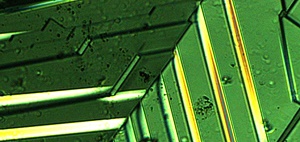
Queen’s researchers have discovered a new way to create extremely thin electrically conducting sheets, which could revolutionise the tiny electronic devices that control everything from smart phones to banking and medical technology.
Through nanotechnology, physicists Dr Raymond McQuaid, Dr Amit Kumar and Professor Marty Gregg from Queen’s University’s School of Mathematics and Physics, have created unique 2D sheets, called domain walls, which exist within crystalline materials.
The sheets are almost as thin as the wonder-material graphene, at just a few atomic layers. However, they can do something that graphene can’t – they can appear, disappear or move around within the crystal, without permanently altering the crystal itself.
Smaller devices
This means that in future, even smaller electronic devices could be created, as electronic circuits could constantly reconfigure themselves to perform a number of tasks, rather than just having a sole function.
Professor Marty Gregg explains: “Almost all aspects of modern life such as communication, healthcare, finance and entertainment rely on microelectronic devices. The demand for more powerful, smaller technology keeps growing, meaning that the tiniest devices are now composed of just a few atoms – a tiny fraction of the width of human hair.”
“As things currently stand, it will become impossible to make these devices any smaller – we will simply run out of space. This is a huge problem for the computing industry and new, radical, disruptive technologies are needed. One solution is to make electronic circuits more ‘flexible’ so that they can exist at one moment for one purpose, but can be completely reconfigured the next moment for another purpose.”
The team’s findings, which have been published in Nature Communications, pave the way for a completely new way of data processing.
Etch-a-sketch
Professor Gregg says: “Our research suggests the possibility to “etch-a-sketch” nanoscale electrical connections, where patterns of electrically conducting wires can be drawn and then wiped away again as often as required.
“In this way, complete electronic circuits could be created and then dynamically reconfigured when needed to carry out a different role, overturning the paradigm that electronic circuits need be fixed components of hardware, typically designed with a dedicated purpose in mind.”
There are two key hurdles to overcome when creating these 2D sheets, long straight walls need to be created. These need to effectively conduct electricity and mimic the behavior of real metallic wires. It is also essential to be able to choose exactly where and when the domain walls appear and to reposition or delete them.
Solutions
Through the research, the Queen’s researchers have discovered some solutions to the hurdles. Their research proves that long conducting sheets can be created by squeezing the crystal at precisely the location they are required, using a targeted acupuncture-like approach with a sharp needle. The sheets can then be moved around within the crystal using applied electric fields to position them.
Dr Raymond McQuaid, a recently appointed lecturer in the School of Mathematics and Physics at Queen’s University, added: “Our team has demonstrated for the first time that copper-chlorine boracite crystals can have straight conducting walls that are hundreds of microns in length and yet only nanometres thick. The key is that, when a needle is pressed into the crystal surface, a jigsaw puzzle-like pattern of structural variants, called “domains”, develops around the contact point. The different pieces of the pattern fit together in a unique way with the result that the conducting walls are found along certain boundaries where they meet.
“We have also shown that these walls can then be moved using applied electric fields, therefore suggesting compatibility with more conventional voltage operated devices. Taken together, these two results are a promising sign for the potential use of conducting walls in reconfigurable nano-electronics.”
Share on:


Suggested Items
Designer’s Notebook: What Designers Need to Know About Manufacturing, Part 2
04/24/2024 | Vern Solberg -- Column: Designer's NotebookThe printed circuit board (PCB) is the primary base element for providing the interconnect platform for mounting and electrically joining electronic components. When assessing PCB design complexity, first consider the component area and board area ratio. If the surface area for the component interface is restricted, it may justify adopting multilayer or multilayer sequential buildup (SBU) PCB fabrication to enable a more efficient sub-surface circuit interconnect.
Insulectro’s 'Storekeepers' Extend Their Welcome to Technology Village at IPC APEX EXPO
04/03/2024 | InsulectroInsulectro, the largest distributor of materials for use in the manufacture of PCBs and printed electronics, welcomes attendees to its TECHNOLOGY VILLAGE during this year’s IPC APEX EXPO at the Anaheim Convention Center, April 9-11, 2024.
ENNOVI Introduces a New Flexible Circuit Production Process for Low Voltage Connectivity in EV Battery Cell Contacting Systems
04/03/2024 | PRNewswireENNOVI, a mobility electrification solutions partner, introduces a more advanced and sustainable way of producing flexible circuits for low voltage signals in electric vehicle (EV) battery cell contacting systems.
Heavy Copper PCBs: Bridging the Gap Between Design and Fabrication, Part 1
04/01/2024 | Yash Sutariya, Saturn Electronics ServicesThey call me Sparky. This is due to my talent for getting shocked by a variety of voltages and because I cannot seem to keep my hands out of power control cabinets. While I do not have the time to throw the knife switch to the off position, that doesn’t stop me from sticking screwdrivers into the fuse boxes. In all honesty, I’m lucky to be alive. Fortunately, I also have a talent for building high-voltage heavy copper circuit boards. Since this is where I spend most of my time, I can guide you through some potential design for manufacturability (DFM) hazards you may encounter with heavy copper design.
Trouble in Your Tank: Supporting IC Substrates and Advanced Packaging, Part 5
03/19/2024 | Michael Carano -- Column: Trouble in Your TankDirect metallization systems based on conductive graphite or carbon dispersion are quickly gaining acceptance worldwide. Indeed, the environmental and productivity gains one can achieve with these processes are outstanding. In today’s highly competitive and litigious environment, direct metallization reduces costs associated with compliance, waste treatment, and legal issues related to chemical exposure. What makes these processes leaders in the direct metallization space?