


 It’s Only Common Sense: OCCAM—the Time Is Now
 Marcy's Musings: The Growing Industry
 Dan’s Biz Bookshelf: Seeing the How
Laying the Foundations for Hybrid Silicon Lasers
June 16, 2017 | A*STAREstimated reading time: 2 minutes
Producing semiconductor lasers on a silicon wafer is a long-held goal for the electronics industry, but their fabrication has proved challenging. Now, researchers at A*STAR have developed an innovative way to manufacture them that is cheap, simple and scalable.
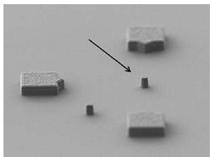
Oblique angle scanning electron microscopy image of a 500 nanometer diameter microdisk.
Hybrid silicon lasers combine the light-emitting properties of group III–V semiconductors, like gallium arsenide and indium phosphide, with the maturity of silicon manufacturing techniques. These lasers are attracting considerable attention as they promise inexpensive, mass-producible optical devices that can integrate with photonic and microelectronic elements on a single silicon chip. They have potential in a wide range of applications, from short-distance data communication to high-speed, long-distance optical transmission.
In the current production process, however, lasers are fabricated on separate III–V semiconductor wafers before being individually aligned to each silicon device — a time-consuming, costly process that limits the number of lasers that can be placed on a chip.
To overcome these limitations, Doris Keh-Ting Ng and her colleagues from the A*STAR Data Storage Institute have developed an innovative method for producing a hybrid III–V semiconductor and silicon-on-insulator (SOI) optical microcavity. This greatly reduces the complexity of the fabrication process and results in a more compact device.
“It’s very challenging to etch the entire cavity,” says Ng. “Currently, there is no single etch recipe and mask that allows the whole microcavity to be etched, and so we decided to develop a new approach.”
By first attaching a thin film of III–V semiconductor to a silicon oxide (SiO2) wafer using a SOI interlayer thermal bonding process, they produced a strong bond that also removes the need for strong oxidizing agents, such as Piranha solution or hydrofluoric acid.
And by using a dual hard-mask technique to etch the microcavity that confined etching to the intended layer, they eliminated the requirement to use multiple overlay lithography and etching cycles — a challenging procedure.
“Our approach cuts down the number of fabrication steps, reduces the use of hazardous chemicals, and requires only one lithography step to complete the process,” explains Ng.
The work presents, for the first time, a new heterocore configuration and integrated fabrication process that combines low-temperature SiO2 interlayer bonding with dual hard-mask, single lithography patterning.
“The process not only makes it possible to produce heterocore devices, it also greatly reduces the challenges of fabricating them, and could serve as an alternative hybrid microcavity for use by the research community,” says Ng.
Share on:


Suggested Items
Designer’s Notebook: What Designers Need to Know About Manufacturing, Part 2
04/24/2024 | Vern Solberg -- Column: Designer's NotebookThe printed circuit board (PCB) is the primary base element for providing the interconnect platform for mounting and electrically joining electronic components. When assessing PCB design complexity, first consider the component area and board area ratio. If the surface area for the component interface is restricted, it may justify adopting multilayer or multilayer sequential buildup (SBU) PCB fabrication to enable a more efficient sub-surface circuit interconnect.
Real Time with... IPC APEX EXPO 2024: Advancements in Laser Depaneling with LPKF
04/24/2024 | Real Time with...IPC APEX EXPOJake Benz, LPKF sales manager for North America, discusses the company's advancements in laser depaneling. LPKF has introduced a green wavelength laser for processing rigid FR-4 circuit boards, bringing significant gains in processing speeds to market. The company transitioned from IR CO2 to UV wavelength due to heat and burning issues.
KYZEN to Focus on AQUANOX A4618 at SMTA Wisconsin Expo & Tech Forum
04/22/2024 | KYZEN'KYZEN, the global leader in innovative environmentally friendly cleaning chemistries, will exhibit at the SMTA Wisconsin Expo & Tech Forum, scheduled to take place Tuesday, May 7, 2024 at the Four Poins by Sheraton, Milwaukee Airport in Milwaukee, WI.
AIM Solder’s Dillon Zhu to Present on Ultraminiature Soldering at SMTA China East
04/22/2024 | AIMAIM Solder, a leading global manufacturer of solder assembly materials for the electronics industry, is pleased to announce that Dillon Zhu will present on the topic: Ultraminiature Soldering: Techniques, Technologies, and Standards at SMTA China East. This event is being held at the Shanghai World Expo Exhibition & Convention Center from April 24-25.
Intel Gaudi, Xeon and AI PC Accelerate Meta Llama 3 GenAI Workloads
04/22/2024 | Intel CorporationMeta launched Meta Llama 3, its next-generation large language model (LLM). Effective on launch day, Intel has validated its AI product portfolio for the first Llama 3 8B and 70B models across Intel® Gaudi® accelerators, Intel® Xeon® processors, Intel® Core™ Ultra processors and Intel® Arc™ graphics.