


 It’s Only Common Sense: OCCAM—the Time Is Now
 Marcy's Musings: The Growing Industry
 Dan’s Biz Bookshelf: Seeing the How
'Magic' Alloy Could Spur Next Generation of Solar Cells
June 20, 2017 | University of MichiganEstimated reading time: 4 minutes
In what could be a major step forward for a new generation of solar cells called "concentrator photovoltaics," University of Michigan researchers have developed a new semiconductor alloy that can capture the near-infrared light located on the leading edge of the visible light spectrum.
Easier to manufacture and at least 25% less costly than previous formulations, it's believed to be the world's most cost-effective material that can capture near-infrared light—and is compatible with the gallium arsenide semiconductors often used in concentrator photovoltaics.
Concentrator photovoltaics gather and focus sunlight onto small, high-efficiency solar cells made of gallium arsenide or germanium semiconductors. They're on track to achieve efficiency rates of over 50%, while conventional flat-panel silicon solar cells top out in the mid-20s.
"Flat-panel silicon is basically maxed out in terms of efficiency," said Rachel Goldman, U-M professor of materials science and engineering, and physics, whose lab developed the alloy. "The cost of silicon isn't going down and efficiency isn't going up. Concentrator photovoltaics could power the next generation."
Varieties of concentrator photovoltaics exist today. They are made of three different semiconductor alloys layered together. Sprayed onto a semiconductor wafer in a process called molecular-beam epitaxy—a bit like spray painting with individual elements—each layer is only a few microns thick. The layers capture different parts of the solar spectrum; light that gets through one layer is captured by the next.
But near-infrared light slips through these cells unharnessed. For years, researchers have been working toward an elusive "fourth layer" alloy that could be sandwiched into cells to capture this light. It's a tall order; the alloy must be cost-effective, stable, durable and sensitive to infrared light, with an atomic structure that matches the other three layers in the solar cell.
Getting all those variables right isn't easy, and until now, researchers have been stuck with prohibitively expensive formulas that use five elements or more.
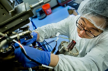
The main growth chamber of the molecular epitaxy beam apparatus in which members of MSE Professor Rachel Goodman's research group characterize various semiconductors in the Gerstacker Building on August 3, 2015. Photo Credit: Joseph XuTo find a simpler mix, Goldman's team devised a novel approach for keeping tabs on the many variables in the process. They combined on-the-ground measurement methods including X-ray diffraction done at U-M and ion beam analysis done at Los Alamos National Laboratory with custom-built computer modeling.
Using this method, they discovered that a slightly different type of arsenic molecule would pair more effectively with the bismuth. They were able to tweak the amount of nitrogen and bismuth in the mix, enabling them to eliminate an additional manufacturing step that previous formulas required. And they found precisely the right temperature that would enable the elements to mix smoothly and stick to the substrate securely.
"'Magic' is not a word we use often as materials scientists," Goldman said. "But that's what it felt like when we finally got it right."
The advance comes on the heels of another innovation from Goldman's lab that simplifies the "doping" process used to tweak the electrical properties of the chemical layers in gallium arsenide semiconductors. During doping, manufacturers apply a mix of chemicals called "designer impurities" to change how semiconductors conduct electricity and give them positive and negative polarity similar to the electrodes of a battery. The doping agents usually used for gallium arsenide semiconductors are silicon on the negative side and beryllium on the positive side.
The beryllium is a problem—it's toxic and it costs about 10 times more than silicon dopants. Beryllium is also sensitive to heat, which limits flexibility during the manufacturing process. But the U-M team discovered that by reducing the amount of arsenic below levels that were previously considered acceptable, they can "flip" the polarity of silicon dopants, enabling them to use the cheaper, safer element for both the
positive and negative sides.
"Being able to change the polarity of the carrier is kind of like atomic 'ambidexterity,'" said Richard Field, a former U-M doctoral student who worked on the project. "Just like people with naturally born ambidexterity, it's fairly uncommon to find atomic impurities with this ability."
Together, the improved doping process and the new alloy could make the semiconductors used in concentrator photovoltaics as much as 30% cheaper to produce, a big step toward making the high-efficiency cells practical for large-scale electricity generation.
"Essentially, this enables us to make these semiconductors with fewer atomic spray cans, and each can is significantly less expensive," Goldman said. "In the manufacturing world, that kind of simplification is very significant. These new alloys and dopants are also more stable, which gives makers more flexibility as the semiconductors move through the manufacturing process."
The new alloy is detailed in a paper titled "Bi-enhanced N incorporation in GaAsNBi alloys," published June 15 in Applied Physics Letters. The research is supported by the National Science Foundation and the U.S. Department of Energy Office of Science Graduate Student Research.
The doping advances are detailed in a paper titled "Influence of surface reconstruction on dopant incorporation and transport properties of GaAs(Bi) alloys." It was published in the Dec. 26, 2016, issue of Applied Physics Letters. The research was supported by the National Science Foundation.
Share on:


Suggested Items
Koh Young Showcases Award-winning Inspection Solutions at SMTconnect with SmartRep in Hall 4A.225
04/25/2024 | Koh Young TechnologyKoh Young Technology, the industry leader in True 3D measurement-based inspection solutions, will showcase an array of award-winning inspection and measurement solutions at SMTconnect alongside its sales partner, SmartRep, in booth 4A.225 at NürnbergMesse from June 11-13, 2023. The following offers a glimpse into what Koh Young will present at the tradeshow:
Real Time with… IPC APEX EXPO 2024: Plasmatreat: Innovative Surface Preparation Solutions
04/25/2024 | Real Time with...IPC APEX EXPOIn this interview, Editor Nolan Johnson speaks with Hardev Grewal, CEO and president of Plasmatreat, a developer of atmospheric plasma solutions. Plasmatreat uses clean compressed air and electricity to create plasma, offering environmentally friendly methods for surface preparation. Their technology measures plasma density for process optimization and can remove organic micro-contamination. Nolan and Hardev also discuss REDOX-Tool, a new technology for removing metal oxides.
KYZEN to Promote Pair of Stencil Cleaning Chemistries at SMTA Ciudad Jaurez Expo & Tech Forum
04/25/2024 | KYZEN'KYZEN, the global leader in innovative environmentally friendly cleaning chemistries, will exhibit at the SMTA Ciudad Juarez Expo & Tech Forum, scheduled to take place Thursday, May 9, 2024 at the Injectronic Convention Center in Ciudad Jaurez, Chihuahua, Mexico. During the event the KYZEN Clean Team will focus on understencil cleaning products KYZEN E5631J and CYBERSOLV C8882.
Cadence, TSMC Collaborate on Wide-Ranging Innovations to Transform System and Semiconductor Design
04/25/2024 | Cadence Design SystemsCadence Design Systems, Inc. and TSMC have extended their longstanding collaboration by announcing a broad range of innovative technology advancements to accelerate design, including developments ranging from 3D-IC and advanced process nodes to design IP and photonics.
Listen Up! The Intricacies of PCB Drilling Detailed in New Podcast Episode
04/25/2024 | I-Connect007In episode 5 of the podcast series, On the Line With: Designing for Reality, Nolan Johnson and Matt Stevenson continue down the manufacturing process, this time focusing on the post-lamination drilling process for PCBs. Matt and Nolan delve into the intricacies of the PCB drilling process, highlighting the importance of hole quality, drill parameters, and design optimization to ensure smooth manufacturing. The conversation covers topics such as drill bit sizes, aspect ratios, vias, challenges in drilling, and ways to enhance efficiency in the drilling department.