


 The Right Approach: I Hear the Train A Comin'
 It’s Only Common Sense: OCCAM—the Time Is Now
 Marcy's Musings: The Growing Industry
Hands off Approach to Looking Into Silicon Chips
June 29, 2017 | London Centre for NanotechnologyEstimated reading time: 2 minutes
The possibility of looking inside silicon chips to see their tiny working parts, without damaging the chips, is a step closer thanks to an international team led by scientists at the LCN.
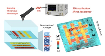
Figure: Microwave Microscope visualizes 3D structures of atomically thin phosphorus layers buried 5-15 nm below a silicon surface
The group at the LCN, led by Dr Neil Curson, have shown that they can generate pictures of tiny three-dimensional components made from phosphorus atoms, that are completely invisible to all other imaging technologies.
Remarkably, the pictures of these components were obtained despite the fact that the components were the size of only a few tens of atoms, were atomically thin and were buried under the surface of the chip. An accurate quantitative determination of the location of the buried components was obtained, along with certain electrical properties. This breakthrough is published in Science Advances.
The components that were studied, including a three-dimensional criss-cross of metallic phosphorus stripes, were designed and manufactured by LCN PhD student Alex Kölker. He used a super-sharp metal needle to write patterns in a single layer of hydrogen atoms that lay on the surface of a silicon chip, creating a template of a desired shape. By causing a chemical reaction to happen between the surface of the chip and phosphine gas, phosphorus atoms were written into the surface, in the shape of the template. The phosphorus structures were then buried with more silicon to complete the device.
A recently developed scanning microwave microscope was used to take pictures of the components, obtained with our collaborators at Johannes Kepler University, led by Georg Gramse, and by Keysight Technologies (Austria), Paul Scherrer Institut, ETH Zürich and EPF Lausanne (Switzerland). The microscope works by focussing microwaves (like those from a microwave oven), to the end of a metal tip which is pushed against the surface of the chip. The microwaves are fired into chip, subsequently bouncing back from the buried components, measured, and used to construct a picture.
According to Dr Curson “The work is potentially of global significance because silicon chips are becoming so sophisticated and intricate that taking snapshots of their smallest working parts is incredibly difficult and time consuming, and currently involves destroying the chip. If we could easily see all components of a chip, in a non-destructive manor, it would be a game-changer. What we have done is a big step towards just that. Such technologies are also becoming important for governments who are interested in knowing what is inside the foreign electronics they are using!”
“Another important application of our imaging technology is in assisting in the fabrication of phosphorus-in-silicon quantum computers, which have the potential to revolutionise computing completely, if realised.”
Dr Ferry Kienberger from Keysight Technologies says “Our company sees this work as a major breakthrough in demonstrating that scanning microwave microscopy is the way forward for the characterisation of the next generation of electrical devices and quantum components in silicon.”
The capabilities demonstrated here are transformative for non-invasive diagnostics of atomic-scale electric components that will form the next generation of “classical” and quantum devices.
Share on:


Suggested Items
IPC Design Competition Champion Crowned at IPC APEX EXPO 2024
04/24/2024 | IPCAt IPC APEX EXPO 2024 in Anaheim, California, five competitors squared off to determine who was the best of the best at PCB design.
Scape Technologies Introduces SCAPE CoCreator at Hannover Messe 2024
04/18/2024 | Scape TechnologiesToday's industrial robotics, 3D Vision, and AI are often confined by costs, complexity, and limited accessibility and usability. Scape Technologies is revolutionizing this field by broadening the horizons of what is possible.
Plasmatreat at IPC APEX EXPO 2024
04/02/2024 | PlasmatreatFor the pretreatment of highly sensitive electronic components, Plasmatreat will present a real innovation at the IPC APEX Expo in Anaheim 2024: The new REDOX tool safely and effectively reduces oxide layers on electronic components in an inline process.
Würth Elektronik Presents LEDs with Integrated Controllers
03/27/2024 | Würth ElektronikWürth Elektronik now offers WL-ICLED, a new series of RGB LEDs with integrated controller (IC). The components, controllable as pixels, combine a red, green and blue LED with a programmable contoller IC.
ROCKA Solutions to Showcase Comprehensive Manufacturing Solutions at the Del Mar Show
03/25/2024 | ROCKA SolutionsROCKA Solutions is excited to announce its participation in the upcoming Del Mar Electronics & Manufacturing Show, scheduled to take place on April 24-25, 2024 at the Del Mar Fairgrounds in San Diego, CA. ROCKA Solutions will be exhibiting in Booth 650, where attendees can learn more about the company's commitment to enhancing supply chains and supporting various manufacturing sectors.