


 It’s Only Common Sense: OCCAM—the Time Is Now
 Marcy's Musings: The Growing Industry
 Dan’s Biz Bookshelf: Seeing the How
Perovskite Photovoltaics Market, 2028
June 30, 2017 | PRNewswireEstimated reading time: 2 minutes
Research and Markets has announced the addition of the "Perovskite Photovoltaics 2018-2028" report to their offering.
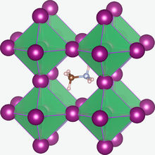
As one of the top ten science breakthroughs of 2013, perovskite solar cells have shown potential both in the rapid efficiency improvement (from 2.2% in 2006 to the latest record 20.1% in 2014) and in cheap material and manufacturing costs. Perovskite solar cells have attracted tremendous attention from the likes of DSSC and OPVs with greater potential. Many companies and research institutes that focused on DSSCs and OPVs now transfer attention to perovskites with few research institutes remaining exclusively committed to OPVs and DSSCs.
Perovskite solar cells are a breath of fresh air into the emerging photovoltaic technology landscape. They have amazed with an incredibly fast efficiency improvement, going from just 2% in 2006 to over 20.1% in 2015.
Photovoltaic (PV) technologies are basically divided into two big categories: wafer-based PV (also called 1st generation PV) and thin-film cell PV.
Traditional crystalline silicon (c-Si) cells (both single crystalline silicon and multi-crystalline silicon) and gallium arsenide (GaAs) cells belong to the wafer-based PVs. Among different single-junction solar technologies, GaAs exhibits the highest efficiency, followed by c-Si cells. The latter dominates the current PV market (about 90% market share).
Thin-film cells normally absorb light 10-100 times more efficiently than silicon, allowing the use of films of just a few microns thick. Cadmium telluride (CdTe) technology has been successfully commercialized, with more than 20% cell efficiency and 17.5% module efficiency record. CdTe cells currently take about 5% of the total market. Other commercial thin-film technologies include hydrogenated amorphous silicon (a-Si:H) and copper indium gallium (di)selenide (CIGS) cells, taking approximately 2% market share each today. Copper zinc tin sulphide technology has been developed for years and it will still require some time for real commercialization.
The emerging thin-film PVs are also called 3rd generation PVs, which refer to PVs using technologies that have the potential to overcome Shockley-Queisser limit or are based on novel semiconductors. The 3rd generation PVs include DSSC, organic photovoltaic (OPV), quantum dot (QD) PV and perovskite PV. The cell efficiencies of perovskite are approaching that of commercialized 2nd generation technologies such as CdTe and CIGS. Other emerging PV technologies are still struggling with lab cell efficiencies lower than 15%.
High and rapidly improved efficiencies, as well as low potential material & processing costs are not the only advantages of perovskite solar cells. Flexibility, semi-transparency, tailored form factors, thin-film, light-weight are other value propositions of perovskite solar cells.
With so many improvements, perovskite solar cell technology is still in the early stages of commercialization compared with other mature solar technologies as there are a number of concerns remaining such as stability, toxicity of lead in the most popular perovskite materials, scaling-up, etc. Crystalline silicon PV modules have fallen from $76.67/W in 1977 to $0.4-0.5/W with fair efficiency in early 2015.
Share on:


Suggested Items
Designer’s Notebook: What Designers Need to Know About Manufacturing, Part 2
04/24/2024 | Vern Solberg -- Column: Designer's NotebookThe printed circuit board (PCB) is the primary base element for providing the interconnect platform for mounting and electrically joining electronic components. When assessing PCB design complexity, first consider the component area and board area ratio. If the surface area for the component interface is restricted, it may justify adopting multilayer or multilayer sequential buildup (SBU) PCB fabrication to enable a more efficient sub-surface circuit interconnect.
Insulectro’s 'Storekeepers' Extend Their Welcome to Technology Village at IPC APEX EXPO
04/03/2024 | InsulectroInsulectro, the largest distributor of materials for use in the manufacture of PCBs and printed electronics, welcomes attendees to its TECHNOLOGY VILLAGE during this year’s IPC APEX EXPO at the Anaheim Convention Center, April 9-11, 2024.
ENNOVI Introduces a New Flexible Circuit Production Process for Low Voltage Connectivity in EV Battery Cell Contacting Systems
04/03/2024 | PRNewswireENNOVI, a mobility electrification solutions partner, introduces a more advanced and sustainable way of producing flexible circuits for low voltage signals in electric vehicle (EV) battery cell contacting systems.
Heavy Copper PCBs: Bridging the Gap Between Design and Fabrication, Part 1
04/01/2024 | Yash Sutariya, Saturn Electronics ServicesThey call me Sparky. This is due to my talent for getting shocked by a variety of voltages and because I cannot seem to keep my hands out of power control cabinets. While I do not have the time to throw the knife switch to the off position, that doesn’t stop me from sticking screwdrivers into the fuse boxes. In all honesty, I’m lucky to be alive. Fortunately, I also have a talent for building high-voltage heavy copper circuit boards. Since this is where I spend most of my time, I can guide you through some potential design for manufacturability (DFM) hazards you may encounter with heavy copper design.
Trouble in Your Tank: Supporting IC Substrates and Advanced Packaging, Part 5
03/19/2024 | Michael Carano -- Column: Trouble in Your TankDirect metallization systems based on conductive graphite or carbon dispersion are quickly gaining acceptance worldwide. Indeed, the environmental and productivity gains one can achieve with these processes are outstanding. In today’s highly competitive and litigious environment, direct metallization reduces costs associated with compliance, waste treatment, and legal issues related to chemical exposure. What makes these processes leaders in the direct metallization space?