


 The Right Approach: I Hear the Train A Comin'
 It’s Only Common Sense: OCCAM—the Time Is Now
 Marcy's Musings: The Growing Industry
Seeing The Invisible With a Graphene-CMOS Integrated Device
July 7, 2017 | Graphene FlagshipEstimated reading time: 2 minutes
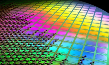
Silicon based CMOS (Complementary metal-oxide semiconductors) technology has truly shaped our world. It enables most of the electronics that we rely on today including computers, smartphones and digital cameras. However, to continue the path of progress in the electronics industry new technology must be developed and a key feature of this is the ability to integrate CMOS with other semiconductors. Now, Graphene Flagship researchers from ICFO (The Institute of Photonic Sciences in Barcelona) have shown that it is possible to integrate graphene into a CMOS integrated circuit.
In their paper published in the journal Nature Photonics they combine this graphene-CMOS device with quantum dots to create an array of photodetectors, producing a high resolution image sensor. When used as a digital camera this device is able to sense UV, visible and infrared light at the same time. This is just one example of how this device might be used, others include in microelectronics, sensor arrays and low-power photonics.
“The development of this monolithic CMOS-based image sensor represents a milestone for low-cost, high-resolution broadband and hyperspectral imaging systems” ICREA Professor at ICFO, Frank Koppens, highlights. He assures that “in general, graphene-CMOS technology will enable a vast amount of applications, that range from safety, security, low cost pocket and smartphone cameras, fire control systems, passive night vision and night surveillance cameras, automotive sensor systems, medical imaging applications, food and pharmaceutical inspection to environmental monitoring, to name a few”.
These results were enabled by the collaboration between Graphene Flagship Partner Graphenea (a Spanish graphene supplier) and ICFO, within the optoelectronics workpackage of the Graphene Flagship.
By creating a hybrid graphene and quantum dot system on a CMOS wafer using a layering and patterning approach, the Flagship team solved a complex problem with a simple solution. First the graphene is deposited, then patterned to define the pixel shape and finally a layer of PbS colloidal quantum dots is added. The photoresponse of this system is based on a photogating effect, which starts as the quantum dot layer absorbs light and transfers it as photo-generated holes or electrons to the graphene, where they circulate due to a bias voltage applied between two pixel contacts. The photo signal is then sensed by the change in conductivity of the graphene, with graphene’s high charge mobility allowing for the high sensitivity of the device.
As Stijn Goossens comments, “No complex material processing or growth processes were required to achieve this graphene-quantum dot CMOS image sensor. It proved easy and cheap to fabricate at room temperature and under ambient conditions, which signifies a considerable decrease in production costs. Even more, because of its properties, it can be easily integrated on flexible substrates as well as CMOS-type integrated circuits.”
The commercial applications of this research and the potential for imaging and sensing technology are now being explored in ICFO’s Launchpad incubator.
Professor Andrea Ferrari, Science and Technology Officer and Chair of the Management Panel of the Graphene Flagship added: "The integration of graphene with CMOS technology is a cornerstone for the future implementation of graphene in consumer electronics. This work is a key first step, clearly demonstrating the feasibility of this approach. The Flagship has put a significant investment in the system level integration of graphene, and this will increase as we move along the technology and innovation roadmap".
Share on:


Suggested Items
Warm Windows and Streamlined Skin Patches – IDTechEx Explores Flexible and Printed Electronics
04/26/2024 | IDTechExFlexible and printed electronics can be integrated into cars and homes to create modern aesthetics that are beneficial and easy to use. From luminous car controls to food labels that communicate the quality of food, the uses of this technology are endless and can upgrade many areas of everyday life.
iNEMI Packaging Tech Topic Series: Role of EDA in Advanced Semiconductor Packaging
04/26/2024 | iNEMIAdvanced semiconductor packaging with heterogenous integration has made on-package integration of multiple chips a crucial part of finding alternatives to transistor scaling. Historically, EDA tools for front-end and back-end design have evolved separately; however, design complexity and the increased number of die-to-die or die-to-substrate interconnections has led to the need for EDA tools that can support integration of overall design planning, implementation, and system analysis in a single cockpit.
Koh Young Showcases Award-winning Inspection Solutions at SMTconnect with SmartRep in Hall 4A.225
04/25/2024 | Koh Young TechnologyKoh Young Technology, the industry leader in True 3D measurement-based inspection solutions, will showcase an array of award-winning inspection and measurement solutions at SMTconnect alongside its sales partner, SmartRep, in booth 4A.225 at NürnbergMesse from June 11-13, 2023. The following offers a glimpse into what Koh Young will present at the tradeshow:
Real Time with… IPC APEX EXPO 2024: Plasmatreat: Innovative Surface Preparation Solutions
04/25/2024 | Real Time with...IPC APEX EXPOIn this interview, Editor Nolan Johnson speaks with Hardev Grewal, CEO and president of Plasmatreat, a developer of atmospheric plasma solutions. Plasmatreat uses clean compressed air and electricity to create plasma, offering environmentally friendly methods for surface preparation. Their technology measures plasma density for process optimization and can remove organic micro-contamination. Nolan and Hardev also discuss REDOX-Tool, a new technology for removing metal oxides.
Nanotechnology Market to Surpass $53.51 Billion by 2031
04/25/2024 | PRNewswireSkyQuest projects that the nanotechnology market will attain a value of USD 53.51 billion by 2031, with a CAGR of 36.4% over the forecast period (2024-2031).