


 The Right Approach: I Hear the Train A Comin'
 It’s Only Common Sense: OCCAM—the Time Is Now
 Marcy's Musings: The Growing Industry
Thin Photodetector Could Increase Performance Without Adding Bulk
July 10, 2017 | University of Wisconsin-MadisonEstimated reading time: 3 minutes
In today’s increasingly powerful electronics, tiny materials are a must as manufacturers seek to increase performance without adding bulk.
Smaller also is better for optoelectronic devices — like camera sensors or solar cells — which collect light and convert it to electrical energy. Think, for example, about reducing the size and weight of a series of solar panels, producing a higher-quality photo in low lighting conditions, or even transmitting data more quickly.
However, two major challenges have stood in the way: First, shrinking the size of conventionally used “amorphous” thin-film materials also reduces their quality. And second, when ultrathin materials become too thin, they become almost transparent and actually lose some ability to gather or absorb light.
Now, in a nanoscale photodetector that combines a unique fabrication method and light-trapping structures, a team of engineers from the University of Wisconsin–Madison and the University at Buffalo has overcome both of those obstacles.
The researchers — electrical engineering professors Zhenqiang (Jack) Ma and Zongfu Yu at UW–Madison and Qiaoqiang Gan at UB — described their device, a single-crystalline germanium nano-membrane photodetector on a nano-cavity substrate, today (July 7, 2017) in the journal Science Advances.
“The idea, basically, is you want to use a very thin material to realize the same function of devices in which you need to use a very thick material,” says Ma.
The device consists of nano-cavities sandwiched between a top layer of ultrathin single-crystal germanium and a reflecting layer of silver.
Tuned to absorb specific light wavelengths, the new photodetector consists of nanocavities sandwiched between a ultrathin single-crystal germanium top layer and reflective silver on the bottom. ILLUSTRATION BY ZHENYANG XIA/UW-MADISON COLLEGE OF ENGINEERING
“Because of the nano-cavities, the photons are ‘recycled’ so light absorption is substantially increased — even in very thin layers of material,” says Ma.
Nano-cavities are made up of an orderly series of tiny, interconnected molecules that essentially reflect, or circulate, light. Gan already has shown that his nano-cavity structures increase the amount of light that thin semiconducting materials like germanium can absorb.
However, most germanium thin films begin as germanium in its amorphous form — meaning the material’s atomic arrangement lacks the regular, repeating order of a crystal. That also means its quality isn’t sufficient for increasingly smaller optoelectronics applications.
That’s where Ma’s expertise comes into play. A world expert in semiconductor nano-membrane devices, Ma used a revolutionary membrane-transfer technology that allows him to easily integrate single crystalline semiconducting materials onto a substrate.
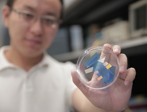
Shrinking photodetectors like this scant wafer held in a frame for testing in the laboratory of UW–Madison engineering Professor Zhenqiang (Jack) Ma help make consumer electronics smaller. STEPHANIE PRECOURT/UW-MADISON COLLEGE OF ENGINEERING
The result is a very thin, yet very effective, light-absorbing photodetector — a building block for the future of optoelectronics.
“It is an enabling technology that allows you to look at a wide variety of optoelectronics that can go to even smaller footprints, smaller sizes,” says Yu, who conducted computational analysis of the detectors.
While the researchers demonstrated their advance using a germanium semiconductor, they also can apply their method to other semiconductors.
“And importantly, by tuning the nano-cavity, we can control what wavelength we actually absorb,” says Gan. “This will open the way to develop lots of different optoelectronic devices.”
The researchers are applying jointly for a patent on the technology through the Wisconsin Alumni Research Foundation. Other authors on the paper include Zhenyang Xia, Munho Kim, Ming Zhou, Tzu-Hsuan Chang, Dong Liu, Xin Yin, Kanglin Xiong, Hongyi Mi and Xudong Wang of UW–Madison; Haomin Song of the University at Buffalo; and Fengnian Xia of Yale University.
Share on:


Suggested Items
SMC Korea 2024 to Highlight Semiconductor Materials Trends and Innovations on Industry’s Path to $1 Trillion
04/24/2024 | SEMIWith Korea a major consumer of semiconductor materials and advanced materials a key driver of innovation on the industry’s path to $1 trillion, industry leaders and experts will gather at SMC (Strategic Materials Conference) Korea 2024 on May 29 at the Suwon Convention Center in Gyeonggi-do, South Korea to provide insights into the latest materials developments and trends. Registration is open.
Groundbreaking Ceremony Marks the Beginning of a New Era for Newccess Industrial; The Construction of the MINGXIN Building
04/12/2024 | Newccess IndustrialOn a clear and sunny day in March, the groundbreaking ceremony for the MINGXIN Building took place in Shenzhen, China. This moment marked the official commencement of construction for a project that will reshape the semiconductor materials industry.
The Need for a Holistic Global Sustainability Standard
04/10/2024 | Michael Ford, Aegis SoftwareNo one can deny that the resources of our fragile planet are finite. The environment seems like a third party, subject to constant degradation. We’re acutely aware of the effects of pollution on our climate, and despite our “throw-away” culture, recycling and recovery of materials has remained relatively expensive, even as we use more energy just to survive.
iNEMI Publishes Four Roadmap Topics
04/04/2024 | iNEMIThe International Electronics Manufacturing Initiative (iNEMI) announces the availability of the first roadmap topics in the new iNEMI Roadmap format. Printed circuit boards, sustainable electronics, smart manufacturing, and mmWave materials and test are now available online.
Insulectro’s 'Storekeepers' Extend Their Welcome to Technology Village at IPC APEX EXPO
04/03/2024 | InsulectroInsulectro, the largest distributor of materials for use in the manufacture of PCBs and printed electronics, welcomes attendees to its TECHNOLOGY VILLAGE during this year’s IPC APEX EXPO at the Anaheim Convention Center, April 9-11, 2024.