


 The Right Approach: I Hear the Train A Comin'
 It’s Only Common Sense: OCCAM—the Time Is Now
 Marcy's Musings: The Growing Industry
Harnessing Hopping Hydrogens for High-Efficiency OLEDS
July 10, 2017 | Kyushu UniversityEstimated reading time: 4 minutes
Renewed investigation of a molecule that was originally synthesized with the goal of creating a unique light-absorbing pigment has led to the establishment of a novel design strategy for efficient light-emitting molecules with applications in next-generation displays and lighting.
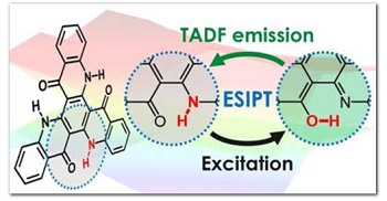
Excited-state intramolecular proton transfer (ESIPT) makes possible organic light-emitting diodes (OLEDs) that are highly efficient by creating the necessary conditions to enable thermally activated delayed fluorescence (TADF). After excitation of the emitting molecule, a hydrogen atom -- technically, just its nucleus -- is transferred to a different atom in the same molecule through a process called ESIPT. The reconfigured molecule can then undergo TADF to convert a high fraction of the excitations into light. Following emission, the molecule returns to its original state. This mechanism increases the molecular design strategies available for the creation of novel and improved light-emitting materials. (Image: William J. Potscavage, Jr.)
Researchers at Kyushu University's Center for Organic Photonics and Electronics Research (OPERA) demonstrated that a molecule that slightly changes its chemical structure before and after emission can achieve a high efficiency in organic light-emitting diodes (OLEDs).
In addition to producing vibrant colors, OLEDs can be fabricated into everything from tiny pixels to large and flexible panels, making them extremely attractive for displays and lighting.
In an OLED, electrical charges injected into thin films of organic molecules come together to form packets of energy - called excitons - that can produce light emission.
The goal is to convert all of the excitons to light, but three-fourths of the created excitons are triplets, which do not produce light in conventional materials, while the remaining one-fourth are singlets, which emit through a process called fluorescence.
Inclusion of a rare metal, such as iridium or platinum, in a molecule can enable rapid emission from the triplets through phosphorescence, which is currently the dominant technology for highly efficient OLEDs.
An alternative mechanism is the use of heat in the environment to give triplets an energetic boost that is sufficient to convert them into light-emitting singlets.
This process, known as thermally activated delayed fluorescence (TADF), easily occurs at room temperature in appropriately designed molecules and has the added advantage of avoiding the cost and reduced molecular design freedom associated with rare metals.
However, most TADF molecules still rely on the same basic design approach.
"Many new TADF molecules are being reported each month, but we keep seeing the same underlying design with electron-donating groups connected to electron-accepting groups," says Masashi Mamada, lead researcher on the study reporting the new results (ACS Central Science, "Highly Efficient Thermally Activated Delayed Fluorescence from an Excited-State Intramolecular Proton Transfer System").
"Finding fundamentally different molecular designs that also exhibit efficient TADF is a key to unlocking new properties, and in this case, we found one by looking at the past with a new perspective."
Currently, combinations of donating and accepting units are primarily used because they provide a relatively simple way to push around the electrons in a molecule and obtain the conditions needed for TADF.
Although the method is effective and a huge variety of combinations is possible, new strategies are still desired in the quest to find perfect or unique emitters.
The mechanism explored by the researchers this time involves the reversible transfer of a hydrogen atom - technically, just its positive nucleus - from one atom in the emitting molecule to another in the same molecule to create an arrangement conducive to TADF.
This transfer occurs spontaneously when the molecule is excited with optical or electrical energy and is known as excited-state intramolecular proton transfer (ESIPT).
This ESIPT process is so important in the investigated molecules that quantum chemical calculations by the researchers indicate that TADF is not possible before transfer of the hydrogen.
After excitation, the hydrogen rapidly transfers to a different atom in the molecule, leading to a molecular structure capable of TADF.
The hydrogen transfers back to its initial atom after the molecule emits light, and the molecule is then ready to repeat the process.
Although TADF from an ESIPT molecule has been reported previously, this is the first demonstration of highly efficient TADF observed inside and outside of a device.
This vastly different design strategy opens the door for achieving TADF with a variety of new chemical structures that would not have been considered based on previous strategies.
Interestingly, the molecule the researchers used was most likely a disappointment when first synthesized nearly 20 years ago by chemists hoping to create a new pigment only to discover that the molecule is colorless.
"Organic molecules never cease to amaze me," says Professor Chihaya Adachi, Director of OPERA. "Many paths with different advantages and disadvantages exist for achieving the same goal, and we have still only scratched the surface of what is possible."
The advantages of this design strategy are just beginning to be explored, but one particularly promising area is related to stability.
Molecules similar to the investigated one are known to be highly resistant to degradation, so researchers hope that these kinds of molecules might help to improve the lifetime of OLEDs.
To see if this is the case, tests are now underway.
While only time will tell how far this particular strategy will go, the continually growing options for OLED emitters certainly bode well for their future.
Share on:


Suggested Items
iNEMI Packaging Tech Topic Series: Role of EDA in Advanced Semiconductor Packaging
04/26/2024 | iNEMIAdvanced semiconductor packaging with heterogenous integration has made on-package integration of multiple chips a crucial part of finding alternatives to transistor scaling. Historically, EDA tools for front-end and back-end design have evolved separately; however, design complexity and the increased number of die-to-die or die-to-substrate interconnections has led to the need for EDA tools that can support integration of overall design planning, implementation, and system analysis in a single cockpit.
Cadence, TSMC Collaborate on Wide-Ranging Innovations to Transform System and Semiconductor Design
04/25/2024 | Cadence Design SystemsCadence Design Systems, Inc. and TSMC have extended their longstanding collaboration by announcing a broad range of innovative technology advancements to accelerate design, including developments ranging from 3D-IC and advanced process nodes to design IP and photonics.
Ansys, TSMC Enable a Multiphysics Platform for Optics and Photonics, Addressing Needs of AI, HPC Silicon Systems
04/25/2024 | PRNewswireAnsys announced a collaboration with TSMC on multiphysics software for TSMC's Compact Universal Photonic Engines (COUPE). COUPE is a cutting-edge Silicon Photonics (SiPh) integration system and Co-Packaged Optics platform that mitigates coupling loss while significantly accelerating chip-to-chip and machine-to-machine communication.
Siemens’ Breakthrough Veloce CS Transforms Emulation and Prototyping with Three Novel Products
04/24/2024 | Siemens Digital Industries SoftwareSiemens Digital Industries Software launched the Veloce™ CS hardware-assisted verification and validation system. In a first for the EDA (Electronic Design Automation) industry, Veloce CS incorporates hardware emulation, enterprise prototyping and software prototyping and is built on two highly advanced integrated circuits (ICs) – Siemens’ new, purpose-built Crystal accelerator chip for emulation and the AMD Versal™ Premium VP1902 FPGA adaptive SoC (System-on-a-chip) for enterprise and software prototyping.
Listen Up! The Intricacies of PCB Drilling Detailed in New Podcast Episode
04/25/2024 | I-Connect007In episode 5 of the podcast series, On the Line With: Designing for Reality, Nolan Johnson and Matt Stevenson continue down the manufacturing process, this time focusing on the post-lamination drilling process for PCBs. Matt and Nolan delve into the intricacies of the PCB drilling process, highlighting the importance of hole quality, drill parameters, and design optimization to ensure smooth manufacturing. The conversation covers topics such as drill bit sizes, aspect ratios, vias, challenges in drilling, and ways to enhance efficiency in the drilling department.