


 It’s Only Common Sense: OCCAM—the Time Is Now
 Marcy's Musings: The Growing Industry
 Dan’s Biz Bookshelf: Seeing the How
Researchers Develop Technique to Control and Measure Electron Spin Voltage
July 14, 2017 | Harvard UniversityEstimated reading time: 3 minutes
Information technologies of the future will likely use electron spin — rather than electron charge — to carry information. But first, scientists need to better understand how to control spin and learn to build the spin equivalent of electronic components, from spin transistors, to spin gates and circuits.
Now, researchers from Harvard University have developed a technique to control and measure spin voltage, known as spin chemical potential. The technique, which uses atomic-sized defects in diamonds to measure chemical potential, is essentially a nanoscale spin multimeter that allows measurements in chip-scale devices.
“There is growing interest in insulating materials that can conduct spin,” said Amir Yacoby, Professor of Physics in the Department of Physics and of Applied Physics at Harvard John A. Paulson School of Engineering and Applied Sciences and senior author of the paper. “Our work develops a new way to look at these spins in materials such as magnets.”
In conducting materials, electrons can carry information by moving from point A to point B. This is an electric current. Spin, on the other hand, can propagate through insulating materials in waves, each electron standing still and communicating spin to its coupled neighbor, like a quantum game of telephone.
To drive these waves from point A to point B, the researchers needed to develop a technique to increase the spin chemical potential — spin voltage — at a local level.
“If you have a high chemical potential at location A and a low chemical potential at location B, spin waves start diffusing from A to B,” said Chunhui Du, a postdoctoral fellow at the Department of Physics and co-first author of the paper. “This is a very important concept in spintronics, because if you are able to control spin-wave transport, then you can use these spin waves instead of electrical current as carriers of information.”
The researchers used two spin-wave injection methods: in the first, they applied fast-oscillating, microwave magnetic fields to excite spin waves. In the second, they converted an electrical current into spin waves using a platinum metal strip located at one end of the magnet.
“What’s remarkable is that this material is an insulator; it doesn’t conduct any current and still you can send information in the form of spin waves through it,” said Toeno Van der Sar, a postdoctoral fellow at the Department of Physics and co-first author of the paper. “Spin waves are so promising because they can travel for a long time without decaying, and there is barely any heat produced because you don’t have moving electrons.”
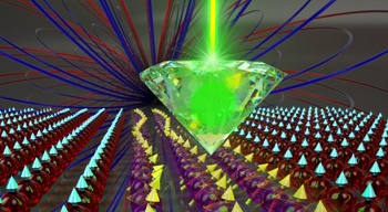
These defects — in which one carbon atom in a diamond is replaced with a nitrogen atom and a neighboring atom is removed — can be used to detect minute magnetic fields.
Tweet This
Once the team injected spin waves into the material, the next step was to figure out how to measure information about those waves. The researchers turned to nitrogen-vacancy (NV) defects in diamonds. These defects — in which one carbon atom in a diamond is replaced with a nitrogen atom and a neighboring atom is removed — can be used to detect minute magnetic fields.
The researchers fabricated tiny rods of diamond containing NV centers and placed them nanometers above the sample. As the spin waves move through the material, they generate a magnetic field, which is picked up by the NV center.
Based on NV-center measurements, researchers can now figure out the spin chemical potential, the number of spin waves, how they are moving through the material and other important insights.
“The nice thing about this technique is that it’s very local,” said Van der Sar. “You can do these measurements just a few nanometers above the sample, which means that you can spatially study the chemical potential in a chip-scale spin-wave device, for let’s say a spin-wave computer. This is not possible with some of the other state–of-the-art techniques.”
This system could also offer a glimpse into more exotic physics such as the spin-wave Hall effect, or show that spin-wave transport is hydrodynamic.
“The principle we use to control and measure the spin chemical potential is quite general. It opens ways to study more exotic spin phenomena in novel materials and aids the development of new spintronic devices,” said Du.
This research was supported in part by the Gordon and Betty Moore Foundation’s Emergent Phenomena in Quantum Systems (EPiQS) Initiative, the Multidisciplinary University Research Initiative (MURI) Quibit Enabled Imaging, Sensing, and Metrology (QuISM) project and the Army Research Office.
Original by: Leah Burrows
Share on:


Suggested Items
SMC Korea 2024 to Highlight Semiconductor Materials Trends and Innovations on Industry’s Path to $1 Trillion
04/24/2024 | SEMIWith Korea a major consumer of semiconductor materials and advanced materials a key driver of innovation on the industry’s path to $1 trillion, industry leaders and experts will gather at SMC (Strategic Materials Conference) Korea 2024 on May 29 at the Suwon Convention Center in Gyeonggi-do, South Korea to provide insights into the latest materials developments and trends. Registration is open.
Groundbreaking Ceremony Marks the Beginning of a New Era for Newccess Industrial; The Construction of the MINGXIN Building
04/12/2024 | Newccess IndustrialOn a clear and sunny day in March, the groundbreaking ceremony for the MINGXIN Building took place in Shenzhen, China. This moment marked the official commencement of construction for a project that will reshape the semiconductor materials industry.
The Need for a Holistic Global Sustainability Standard
04/10/2024 | Michael Ford, Aegis SoftwareNo one can deny that the resources of our fragile planet are finite. The environment seems like a third party, subject to constant degradation. We’re acutely aware of the effects of pollution on our climate, and despite our “throw-away” culture, recycling and recovery of materials has remained relatively expensive, even as we use more energy just to survive.
iNEMI Publishes Four Roadmap Topics
04/04/2024 | iNEMIThe International Electronics Manufacturing Initiative (iNEMI) announces the availability of the first roadmap topics in the new iNEMI Roadmap format. Printed circuit boards, sustainable electronics, smart manufacturing, and mmWave materials and test are now available online.
Insulectro’s 'Storekeepers' Extend Their Welcome to Technology Village at IPC APEX EXPO
04/03/2024 | InsulectroInsulectro, the largest distributor of materials for use in the manufacture of PCBs and printed electronics, welcomes attendees to its TECHNOLOGY VILLAGE during this year’s IPC APEX EXPO at the Anaheim Convention Center, April 9-11, 2024.