


 It’s Only Common Sense: OCCAM—the Time Is Now
 Marcy's Musings: The Growing Industry
 Dan’s Biz Bookshelf: Seeing the How
New Method Promises Easier Nanoscale Manufacturing
July 28, 2017 | University of ChicagoEstimated reading time: 2 minutes
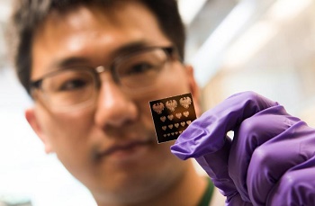
Scientists at the University of Chicago and Argonne National Laboratory have discovered a new way to precisely pattern nanomaterials that could open a new path to the next generation of everyday electronic devices.
The new research, published in Science, is expected to make such materials easily available for eventual use in everything from LED displays to cellular phones to photodetectors and solar cells. Though nanomaterials are promising for future devices, ways to build them into complex structures have been limited and small-scale.
“This is a step needed to move quantum dots and many other nanomaterials from proof-of-concept experiments to real technology we can use,” said co-author Dmitri Talapin, professor of chemistry at UChicago and a scientist with the Center for Nanoscale Materials at Argonne. “It really expands our horizons.”
Examples of optically patterned inorganic materials. The top row demonstrates negative patterning, and the bottom row demonstrates positive patterning. Courtesy ofDmitri Talapin and Yuanyuan Wang / Illustration by UChicago Creative
The foundation of modern computing is a tiny switch called the transistor, made billions at a time by a technique called photolithography. This process, which has made smartphones cheap and ubiquitous, carves a stencil out of a layer of organic polymer by laying down a patterned “mask” and illuminating it with ultraviolet light. After the new material is deposited on top, the polymer stencil is lifted off to reveal the pattern. Several rounds of such patterning build a miniature transistor onto the material.
But the method has its limitations. Only a few materials can be patterned this way; it was originally developed for silicon, and as silicon’s half-century reign over electronics reaches its end, scientists are looking ahead to the next materials.
One such avenue of interest is nanomaterials—tiny crystals of metals or semiconductors. At this scale, they can have unique and useful properties, but manufacturing devices out of them has been difficult.
The new technique, called DOLFIN, makes different nanomaterials directly into “ink” in a process that bypasses the need to lay down a polymer stencil. Talapin and his team carefully designed chemical coatings for individual particles. These coatings react with light, so if you shine light through a patterned mask, the light will transfer the pattern directly into the layer of nanoparticles below—wiring them into useful devices.
“We found the quality of the patterns was comparable to those made with state-of-the-art techniques,” said lead author Yuanyuan Wang, postdoctoral researcher at UChicago. “It can be used with a wide range of materials, including semiconductors, metals, oxides or magnetic materials—all commonly used in electronics manufacturing.”
Share on:


Suggested Items
Groundbreaking Ceremony Marks the Beginning of a New Era for Newccess Industrial; The Construction of the MINGXIN Building
04/12/2024 | Newccess IndustrialOn a clear and sunny day in March, the groundbreaking ceremony for the MINGXIN Building took place in Shenzhen, China. This moment marked the official commencement of construction for a project that will reshape the semiconductor materials industry.
The Need for a Holistic Global Sustainability Standard
04/10/2024 | Michael Ford, Aegis SoftwareNo one can deny that the resources of our fragile planet are finite. The environment seems like a third party, subject to constant degradation. We’re acutely aware of the effects of pollution on our climate, and despite our “throw-away” culture, recycling and recovery of materials has remained relatively expensive, even as we use more energy just to survive.
iNEMI Publishes Four Roadmap Topics
04/04/2024 | iNEMIThe International Electronics Manufacturing Initiative (iNEMI) announces the availability of the first roadmap topics in the new iNEMI Roadmap format. Printed circuit boards, sustainable electronics, smart manufacturing, and mmWave materials and test are now available online.
Insulectro’s 'Storekeepers' Extend Their Welcome to Technology Village at IPC APEX EXPO
04/03/2024 | InsulectroInsulectro, the largest distributor of materials for use in the manufacture of PCBs and printed electronics, welcomes attendees to its TECHNOLOGY VILLAGE during this year’s IPC APEX EXPO at the Anaheim Convention Center, April 9-11, 2024.
Checking In With ICAPE Group
04/03/2024 | Nolan Johnson, I-Connect007ICAPE Group’s field application engineer Erik Pederson drills down on sustainability, supply chain resiliency, and what value engineering really looks like in this exclusive interview. Founded in 1999, European-based ICAPE Group provides 21 million printed circuit boards and over six million technical parts to manufacturers every month. With 30 PCB manufacturing partners globally and 50 partners providing a wide array of technical parts, ICAPE Group has operations in China, Taiwan, Thailand, South Korea, Vietnam, South Africa, Europe, Mexico, and the United States. The company also focuses on the value proposition for its customers.