


 It’s Only Common Sense: OCCAM—the Time Is Now
 Marcy's Musings: The Growing Industry
 Dan’s Biz Bookshelf: Seeing the How
2D Materials Clean Up Their Act
August 2, 2017 | University of ManchesterEstimated reading time: 2 minutes
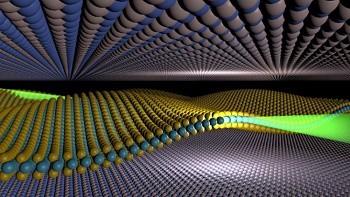
Two-dimensional materials such as graphene may only be one or two atoms thick but they are poised to power flexible electronics, revolutionize composites and even clean our water.
However, being this thin comes at a price: the functional properties we depend on will change if the material becomes contaminated.
Luckily, many 2D materials exhibit the ‘self-cleaning phenomenon’, meaning when different 2D materials are pressed together, stray molecules from the air and the lab are pushed out leaving large areas clear of impurities.
Since graphene’s isolation in 2004 a whole host of other 2D materials have been discovered each with a range of different properties.
When graphene and other 2D materials are combined, the potential of these new materials comes alive.
Layering stacks of 2D materials in a precisely chosen sequence can produce new materials called heterostructures that can be fine-tuned to achieve a specific purpose (from LEDs, to water purification, to high speed electronics).
These flat regions have yielded some of the most fascinating physics of our time. Now, the assumption that these areas are completely clean is under scrutiny.
Writing in Nano Letters a team of researchers at the National Graphene Institute at The University of Manchester have shown that even the gas within which the 2D material stacks are assembled can affect the structure and properties of the materials.
They found that for one class of 2D materials called the transition metal dichalcogenides (TMDCs), some had a very large gap between them and their neighbour; a distance unexplained by theoretical calculations done by Professsor Katsnelson and Dr Rudenko at Radboud University, Netherlands.
These observations all seemed to point to the presence of impurities between the 2D materials. To confirm this, 2D materials were stacked in a pure Argon gas atmosphere using a sealed chamber (known as a glove-box) in which the environment can be completely controlled.
Where previously the same material had given large gaps between neighbours, this time gave distances matching those predicted by theory for a clean interface free from impurities.
“By taking a side view of these sandwich structures we can see how these unique materials stick together and discover new secrets we have previously missed.”
Dr Sarah Haigh, who led the team of researchers who carried out this work said: “This sort of insight is changing how we build devices like LEDs and sensors from 2D materials. The properties of these devices were known to depend heavily on how and where we make them, and for the first time we have observed why.”
The consequences of this finding will directly impact on how we make graphene devices for future applications, showing that even the environment within which 2D material stacks are assembled affects the atomic structure and properties.
This research was funded by the UK Engineering and Physical Sciences Research Council (EPSRC) and its NOWNANO Doctoral Training Centre, the Royal Society, the US Defense Threat Reduction Agency, and ERC starter grant EvoluTEM.
Related video:
Share on:


Suggested Items
Groundbreaking Ceremony Marks the Beginning of a New Era for Newccess Industrial; The Construction of the MINGXIN Building
04/12/2024 | Newccess IndustrialOn a clear and sunny day in March, the groundbreaking ceremony for the MINGXIN Building took place in Shenzhen, China. This moment marked the official commencement of construction for a project that will reshape the semiconductor materials industry.
The Need for a Holistic Global Sustainability Standard
04/10/2024 | Michael Ford, Aegis SoftwareNo one can deny that the resources of our fragile planet are finite. The environment seems like a third party, subject to constant degradation. We’re acutely aware of the effects of pollution on our climate, and despite our “throw-away” culture, recycling and recovery of materials has remained relatively expensive, even as we use more energy just to survive.
iNEMI Publishes Four Roadmap Topics
04/04/2024 | iNEMIThe International Electronics Manufacturing Initiative (iNEMI) announces the availability of the first roadmap topics in the new iNEMI Roadmap format. Printed circuit boards, sustainable electronics, smart manufacturing, and mmWave materials and test are now available online.
Insulectro’s 'Storekeepers' Extend Their Welcome to Technology Village at IPC APEX EXPO
04/03/2024 | InsulectroInsulectro, the largest distributor of materials for use in the manufacture of PCBs and printed electronics, welcomes attendees to its TECHNOLOGY VILLAGE during this year’s IPC APEX EXPO at the Anaheim Convention Center, April 9-11, 2024.
Checking In With ICAPE Group
04/03/2024 | Nolan Johnson, I-Connect007ICAPE Group’s field application engineer Erik Pederson drills down on sustainability, supply chain resiliency, and what value engineering really looks like in this exclusive interview. Founded in 1999, European-based ICAPE Group provides 21 million printed circuit boards and over six million technical parts to manufacturers every month. With 30 PCB manufacturing partners globally and 50 partners providing a wide array of technical parts, ICAPE Group has operations in China, Taiwan, Thailand, South Korea, Vietnam, South Africa, Europe, Mexico, and the United States. The company also focuses on the value proposition for its customers.