


 The Right Approach: I Hear the Train A Comin'
 It’s Only Common Sense: OCCAM—the Time Is Now
 Marcy's Musings: The Growing Industry
Researchers Explore Graphene’s Potential Use in Nanotechnology
August 18, 2017 | Carnegie Mellon UniversityEstimated reading time: 2 minutes
Carnegie Mellon University’s Ge Yang, associate professor of biomedical engineering (BME) and computational biology, and Tzahi Cohen-Karni, assistant professor of BME and materials science and engineering, have determined that graphene is safe for neurons and non-neuronal cells and has long-term biocompatibility — making it an excellent material to use in devices that interface with the nervous system. In a separate study, Cohen-Karni also found it was possible to grow graphene “fuzz.”
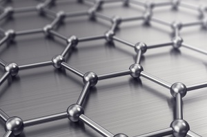
Graphene is nearly 200 times stronger than steel, flexible, nearly transparent and highly conductive. Since graphene is a single layer of carbon atoms connected in a hexagonal pattern, it is thin and lightweight, making it attractive for nanotechnology applications such as building nanodevices for biomedical applications.
Following this new finding, the research team will begin to use graphene with different types of tissues to better understand cell physiology.
Yang, who studies material transport in neurons, is working to better understand brains on the cellular level to improve treatment of neurodegenerative diseases.
“The potential of using graphene to build devices that interact with neurons is amazing because of all of the interesting traits of the material,” Yang said. “The transparency allows you to shine lights through the graphene so that you can use optics to visualize and control chemical signals inside the cell. And because graphene is incredibly conductive, you can simultaneously do sensitive recordings of electrical signals of the neurons.”
Graphene’s ability to store electric charges is attracting the attention of technologies. This feature is largely derived from graphene’s high amount of surface area relative to its volume.
Cohen-Karni’s team was successful in growing graphene in 3-D by first creating a mesh of nanowires made of silicon, which acted as a surface for the graphene to grow on. Then, the team exposed the mesh to methane plasma, which resulted in carbon separating from the methane and depositing onto the mesh, forming graphene.
After using various levels of methane plasma and letting the mesh “cook” for various lengths of time, Cohen-Karni’s team began to see tiny flakes or “fuzz” of graphene growing off the surface of the silicon nanowires. Unlike previous studies, the graphene was growing in three dimensions.
“Until this study, all of the graphene that people have grown are pinned to a surface — it exposes 2-D topology, and you don’t get the advantage of high surface-to-volume ratio that one could achieve if it were grown in 3-D,” Cohen-Karni said. “High surface-to-volume is necessary to make thin-film supercapacitors that can be used in miniaturized circuits.”
Supercapacitors are devices that are able to store and deliver electric charge much, much faster than batteries.
“Imagine a self-sustained system, where the power is supplied to the nanosensing unit from 3-D graphene-based super capacitors,” Cohen-Karni said. “Someday we could have sensors that measure hormone or toxin levels, and you’d never have to replace the battery.”
Share on:


Suggested Items
Real Time with… IPC APEX EXPO 2024: Exploring the Future of Surface Finishes
04/25/2024 | Real Time with...IPC APEX EXPOJoe McGurran, product marketing director for MKS Atotech, looks into the future of surface finishes, discussing less nickel, reduced thickness, technologies influencing HDI and UHDI, and the benefits of nickel-free surface finishes. He also touches on popular finishes like ENIG and palladium immersion gold and discusses the value proposition of making a change.
Designer’s Notebook: What Designers Need to Know About Manufacturing, Part 2
04/24/2024 | Vern Solberg -- Column: Designer's NotebookThe printed circuit board (PCB) is the primary base element for providing the interconnect platform for mounting and electrically joining electronic components. When assessing PCB design complexity, first consider the component area and board area ratio. If the surface area for the component interface is restricted, it may justify adopting multilayer or multilayer sequential buildup (SBU) PCB fabrication to enable a more efficient sub-surface circuit interconnect.
IDTechEx Report Unveils 3D Electronics Status and Opportunities
04/22/2024 | PRNewswire3D electronics is an emerging manufacturing approach that enables electronics to be integrated within or onto the surface of objects. 3D electronic manufacturing techniques empower new features, including mass customizability, greater integration, and improved sustainability in the electronics industry.
NASA, Japan Advance Space Cooperation, Sign Agreement for Lunar Rover
04/11/2024 | NASANASA Administrator Bill Nelson and Japan’s Minister of Education, Culture, Sports, Science and Technology (MEXT) Masahito Moriyama have signed an agreement to advance sustainable human exploration of the Moon.
Lockheed Martin Conducts Historic LRASM Flight Test
04/04/2024 | Lockheed MartinThe U.S. Navy in partnership with Lockheed Martin [NYSE: LMT] successfully conducted a historic Long-Range Anti-Ship Missile (LRASM) flight test with four missiles simultaneously in flight.