


 The Right Approach: I Hear the Train A Comin'
 It’s Only Common Sense: OCCAM—the Time Is Now
 Marcy's Musings: The Growing Industry
Nanotechnology Moves From the Clean Room to the Classroom
August 21, 2017 | Argonne National LaboratoryEstimated reading time: 3 minutes
For years, scientists have been creating and tweaking extremely tiny materials atom by atom in special clean rooms scrubbed of debris. Students needed a Ph.D. to join the club and study those tiny materials in a field known as nanoscience.
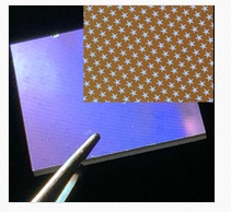
Today, high school students can dabble in nanoscience thanks to the U.S. Department of Energy’s Argonne National Laboratory and industry partner United Scientific Supplies, Inc. High school students can get a hands-on introduction to nanoscience by growing copper wires at the nano-scale (one billionth of a meter) and micro-scale (millionth of a meter) using technology developed at Argonne’s Center for Nanoscale Materials, a DOE Office of Science User Facility, and produced by United Scientific.
“United Scientific is always on the lookout for interesting science breakthroughs that can be developed into new products for schools,” said Raj Soni, president of United Scientific Supplies. “We have long admired the work being done at Argonne and are pleased to make teachers and students aware of cutting-edge research in nanotechnology developed at the Center for Nanoscale Materials.”
With United’s Nanotechnology NextGen STEM Kit, students can grow pattern-shaped wires or structures using Argonne’s patented ultra-nanocrystalline diamond technology. The wires become the essential components to fabricate optical and electrical sensors, similar to the technology used in pressure sensors and other simple devices, in a matter of a few minutes.
Students are able to build micro/nanowires quickly and visualize the wires using an optical microscope, a standard tool in most high school science labs.
“When I was in high school, I was eager to explore inside the science lab,” said Anirudha Sumant, materials scientist at the Center for Nanoscale Materials. “I’d like to inspire that same excitement and eagerness by providing students with accessible, hands-on lab experiments that can draw their attention and stimulate critical thinking.”
The opportunity came when chemist Mike Zach, former Center for Nanoscale Materials facility user and current researcher at Oak Ridge National Laboratory, approached Sumant to develop a simple electrochemical method to mass produce micro- and nanowires. Sumant and Zach developed a process based on Argonne’s technology to adhere metal nanowires, in various shapes and configurations, on a reusable diamond template after simply removing the wires with clear tape. Students can use it again and again since diamond is chemically inert and does not strongly adhere to metals.
Sumant and Zach’s first version of the kit, NanoFabLab In a Box, won two awards in 2014 — an R&D 100 Award and a NASA Brief Tech Magazine Award.
Both partners believe the kit can boost students’ interest in science, technology, engineering and math (STEM) careers.
“The nanotechnology kit is available to teachers through our network of science products dealers across the United States,” said Soni. “Most components are designed for repeated classroom use.”
United Scientific is planning to continue work with Argonne to develop another NextGen STEM kit in the near future.
“Argonne’s Center for Nanoscale Materials is committed to groundbreaking science and inspiring the next generation of researchers,” said Center for Nanoscale Materials Director Supratik Guha.
About Argonne’s Center for Nanoscale Materials
The Center for Nanoscale Materials at Argonne National Laboratory is one of the five DOE Nanoscale Science Research Centers (NSRCs), premier national user facilities for interdisciplinary research at the nanoscale, supported by the DOE Office of Science. Together, the NSRCs comprise a suite of complementary facilities that provide researchers with state-of-the-art capabilities to fabricate, process, characterize and model nanoscale materials, and constitute the largest infrastructure investment of the National Nanotechnology Initiative. The NSRCs are located at DOE’s Argonne, Brookhaven, Lawrence Berkeley, Oak Ridge and Sandia and Los Alamos National Laboratories.
Share on:


Suggested Items
Designer’s Notebook: What Designers Need to Know About Manufacturing, Part 2
04/24/2024 | Vern Solberg -- Column: Designer's NotebookThe printed circuit board (PCB) is the primary base element for providing the interconnect platform for mounting and electrically joining electronic components. When assessing PCB design complexity, first consider the component area and board area ratio. If the surface area for the component interface is restricted, it may justify adopting multilayer or multilayer sequential buildup (SBU) PCB fabrication to enable a more efficient sub-surface circuit interconnect.
Insulectro’s 'Storekeepers' Extend Their Welcome to Technology Village at IPC APEX EXPO
04/03/2024 | InsulectroInsulectro, the largest distributor of materials for use in the manufacture of PCBs and printed electronics, welcomes attendees to its TECHNOLOGY VILLAGE during this year’s IPC APEX EXPO at the Anaheim Convention Center, April 9-11, 2024.
ENNOVI Introduces a New Flexible Circuit Production Process for Low Voltage Connectivity in EV Battery Cell Contacting Systems
04/03/2024 | PRNewswireENNOVI, a mobility electrification solutions partner, introduces a more advanced and sustainable way of producing flexible circuits for low voltage signals in electric vehicle (EV) battery cell contacting systems.
Heavy Copper PCBs: Bridging the Gap Between Design and Fabrication, Part 1
04/01/2024 | Yash Sutariya, Saturn Electronics ServicesThey call me Sparky. This is due to my talent for getting shocked by a variety of voltages and because I cannot seem to keep my hands out of power control cabinets. While I do not have the time to throw the knife switch to the off position, that doesn’t stop me from sticking screwdrivers into the fuse boxes. In all honesty, I’m lucky to be alive. Fortunately, I also have a talent for building high-voltage heavy copper circuit boards. Since this is where I spend most of my time, I can guide you through some potential design for manufacturability (DFM) hazards you may encounter with heavy copper design.
Trouble in Your Tank: Supporting IC Substrates and Advanced Packaging, Part 5
03/19/2024 | Michael Carano -- Column: Trouble in Your TankDirect metallization systems based on conductive graphite or carbon dispersion are quickly gaining acceptance worldwide. Indeed, the environmental and productivity gains one can achieve with these processes are outstanding. In today’s highly competitive and litigious environment, direct metallization reduces costs associated with compliance, waste treatment, and legal issues related to chemical exposure. What makes these processes leaders in the direct metallization space?