


 The Right Approach: I Hear the Train A Comin'
 It’s Only Common Sense: OCCAM—the Time Is Now
 Marcy's Musings: The Growing Industry
New Terahertz Imaging Approach Could Speed Up Skin Cancer Detection
August 24, 2017 | OSAEstimated reading time: 5 minutes
Researchers have developed a new terahertz imaging approach that, for the first time, can acquire micron-scale resolution images while retaining computational approaches designed to speed up image acquisition. This combination could allow terahertz imaging to be useful for detecting early-stage skin cancer without requiring a tissue biopsy from the patient.
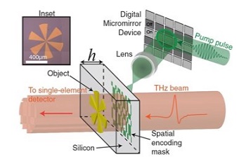
To enable high resolution terahertz imaging, the researchers used a digital micromirror device to project laser light onto a silicon wafer in a specific pattern. When a terahertz beam passes through the wafer, a computer can reconstruct an image of the object based on the pattern of terahertz light detected. The inset shows an optical image of the test target (gold pinwheel) on a 6-mm thick silicon wafer. Image Credit: Rayko Stantchev, University of Exeter.
Terahertz wavelengths fall between microwaves and infrared light on the electromagnetic spectrum. Light in this region is ideal for biological applications because, unlike x-rays, it doesn’t carry enough energy to harm tissue. Other research has shown that skin cancer cells absorb terahertz light more strongly than healthy cells, demonstrating that terahertz imaging can be useful for distinguishing between cancerous and healthy tissue.
“Skin cancer can already be detected using terahertz light, but because of the low resolution of current imaging approaches, the cancer can only be seen after it has grown quite large,” said the research team’s leader, Rayko Stantchev of the University of Exeter, UK. “Ideally, we want to detect the cancer early, when it is still small. We hope that high-resolution terahertz images, combined with the ability to take an image quickly, could eventually lead to a device that could detect cancer in the doctor’s office.”
In Optica, The Optical Society's journal for high impact research, the researchers showed that their near-field approach to terahertz imaging can achieve a spatial resolution of about nine microns and was compatible with compressed sensing and adaptive imaging algorithms that allow three times faster image acquisition than conventional technologies.
In addition to its practical benefits for medical imaging, the research also represents a new way of accomplishing high resolution terahertz imaging. In conventional imaging, spatial resolution is limited by the diffraction limit, which is determined by the wavelength of light used. Although most imaging techniques detect scattered light at some distance from the object being imaged, the researchers overcame the diffraction limit by using a unique setup to measure close, or near-field, interactions of terahertz waves with the object being imaged. Their approach produced a resolution about 1/45 of the wavelength used for imaging.
“This is the first experimental demonstration, for any spectral region, showing that compressed sensing and adaptive imaging can be performed at resolutions much smaller than the wavelength of light used for imaging,” said Stantchev. “Showing that this is physically possible will allow engineers and scientists to start to think about the full potential of this approach.”
Subwavelength terahertz imaging
The primary innovation that made the new approach possible was a digital micromirror device (DMD), an array of tiny mirrors that can each be controlled by a computer. The researchers use the DMD to project a pattern of 800nm light onto a silicon wafer, which makes the wafer opaque to terahertz light in areas where the 800nm light hits the silicon. This means that when a terahertz beam passes though the wafer, it creates a patterned terahertz beam on the other side of the wafer that can then interact with an object being imaged. Because the pattern created by the DMD is known, a computer can reconstruct an image of the object based on the detected terahertz light.
Because near-field terahertz imaging approaches are typically plagued by slow acquisition speeds, the researchers designed their approach to be compatible with compressed sensing and adaptive sampling algorithms that increase the rate of imaging. These algorithms work similarly to image compression, which reduces the size of an image by getting rid of any data not needed to visually perceive an image. Compressed sensing and adaptive imaging algorithms take this a step farther by ignoring the unnecessary data to begin with, speeding up imaging by measuring only the vital components of the image.
“We used these algorithms to determine which regions of the wafer are transparent and which regions are not transparent, essentially creating pixels,” said Stantchev. “Because we were using a single-pixel terahertz detector, normally each pixel would acquire one measurement. However, by creating many transparent pixels in one measurement, an image can be acquired more quickly by taking fewer measurements than the number of pixels.”
The researchers used their setup to image a variety of objects and showed that the method could distinguish arms of a metallic cartwheel that were spaced about nine microns apart.
Moving towards practicality
“For our current setup, we have to use a very intense laser to make the silicon wafers opaque,” said Stantchev. “This laser is very big and expensive, so to make this approach practical we needed to figure out how to do it using a much cheaper and smaller laser.”
Stantchev is now working with researchers in the Chinese University of Hong Kong who have created a different optical setup that might be able to make the silicon wafers opaque using a less powerful laser. The researchers are now working together to see if this approach might make it possible to acquire subwavelength terahertz images using a laser that cost around $200 instead of the almost $400,000 laser used for the work reported in the Optica paper.
“This is one step toward making the technique more compatible with biological applications,” said Stantchev. “Eventually, we envision a device that could be used in the doctor’s office that would quickly reveal if skin cancer is present.”
About Optica
Optica is an open-access, online-only journal dedicated to the rapid dissemination of high-impact peer-reviewed research across the entire spectrum of optics and photonics. Published monthly by The Optical Society (OSA), Optica provides a forum for pioneering research to be swiftly accessed by the international community, whether that research is theoretical or experimental, fundamental or applied. Optica maintains a distinguished editorial board of more than 40 associate editors from around the world and is overseen by Editor-in-Chief Alex Gaeta, Columbia University, USA. For more information, visit Optica.
About The Optical Society
Founded in 1916, The Optical Society (OSA) is the leading professional organization for scientists, engineers, students and business leaders who fuel discoveries, shape real-life applications and accelerate achievements in the science of light. Through world-renowned publications, meetings and membership initiatives, OSA provides quality research, inspired interactions and dedicated resources for its extensive global network of optics and photonics experts. For more information, visit osa.org.
Share on:


Suggested Items
Inkjet Solder Mask ‘Has Arrived’
04/10/2024 | Pete Starkey, I-Connect007I was delighted to be invited to attend an interactive webinar entitled “Solder Mask Coating Made Easy with Additive Manufacturing,” hosted by SUSS MicroTec Netherlands in Eindhoven. The webinar was introduced and moderated by André Bodegom, managing director at Adeon Technologies, and the speakers were Mariana Van Dam, senior product manager PCB imaging solutions at AGFA in Belgium; Ashley Steers, sales manager at Electra Polymers in the UK; and Dr. Luca Gautero, product manager at SUSS MicroTec Netherlands.
NetVia Group Acquires Direct Imaging from Mivatek
04/09/2024 | Miva TechnologiesMiva Technologies is pleased to announce NetVia Group, Irving, TX has acquired a new Miva 2400NG Dual Tray Direct Imaging System with 30-micron capabilities for inner, outer and soldermask imaging.
Teledyne to Acquire Adimec
02/13/2024 | TeledyneTeledyne Technologies Incorporated announced that it has entered into an agreement to acquire Adimec Holding B.V. and its subsidiaries.
Real Time with... productronica 2023: MivaTek Global Advances Technology With High-res Imaging System
12/08/2023 | Real Time with...productronicaMivaTek's Brendan Hogan talks about how the company employs Digitally Adaptive Rasterization Technology (DART) in their high-res imaging equipment. He also shares how the blurred line between semiconductors and microelectronics is driving broader application of the imaging process.
Keysight Enables Validation of Arbe 4D Imaging Radar Chipset
11/30/2023 | Keysight Technologies, Inc.Keysight Technologies, Inc. announces that Arbe has selected the E8719A Radar Target Solution (RTS) to test the Arbe 4D imaging radar chipset for automotive applications.