


 It’s Only Common Sense: OCCAM—the Time Is Now
 Marcy's Musings: The Growing Industry
 Dan’s Biz Bookshelf: Seeing the How
Microfluidics: A Better Bond With Less Bubbling
August 25, 2017 | A*STAREstimated reading time: 2 minutes
Microfluidics technology could revolutionize point-of-care medicine by making it possible to fabricate cheap, disposable card-sized plastic ‘microfluidic chips’ capable of diagnosing a range of conditions on the spot from a drop of blood. A simple bonding technique could help to make this a reality.
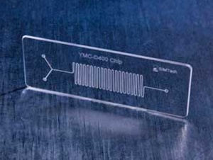
Microfluidic chips make it possible to analyse a drop of blood almost instantly and have the potential to revolutionize healthcare. (Image: A*STAR Singapore Institute of Manufacturing Technology)
This technology has been under development for many years, but has been hampered by the difficult and expensive task of bonding the plastic parts of the chips in a way that preserves the integrity of the microchannels needed to achieve diagnostic functions.
Now a bonding technique that overcomes many of the shortcomings of existing bonding methods has been developed by researchers from A*STAR’s Singapore Institute of Manufacturing Technology (SIMTech) in collaboration with coworkers from Nanyang Technological University and Seoul National University of Science and Technology (Journal of Materials Processing Technology, "Micro-ultrasonic welding using thermoplastic-elastomeric composite film").
“A key challenge in the commercialization of microfluidic devices is lowering the manufacturing cost,” explains Gary Sum Huan Ng from the SIMTech team. “The bonding process to seal the microchannels is often the bottleneck in microfluidics manufacturing.”
Microfluidic devices are essentially comprised of microchannels etched into plastic, which route a sample of biofluid to reservoirs of fluids or substrates that are active toward an analyte that may be present in the sample.
Many methods are used to bond the various parts of a microfluidic device together, but most are slow and painstaking, hindering mass production. Ultrasonic welding, which applies high-frequency vibrations to create a solid-state weld, is promising for scaling up production because it’s fast, produces a strong bond, and uses compact automated equipment. However, the quality of bonds produced by ultrasonic welding is difficult to control due to excess melting and the entrapment of air bubbles.
The researchers have shown that sandwiching a composite film between the two plastic parts to be bonded is very effective in preventing air bubbles and melt flow during ultrasonic welding. The key was to incorporate thermoplastic microspheres in the composite film to help confine and control melting.
“The thermoplastic microspheres, which are scattered within an elastomer matrix to form the composite film, act as micro energy directors that melt and collapse when the ultrasonic energy is applied to create the weld,” says Ng. “The ultrasonic directors are restrained by the elastomeric matrix, which effectively prevents uncontrolled melt flow as well as the generation of trapped air bubbles. This method may overcome the critical bonding issue in the mass manufacturing of microfluidic devices.”
Share on:


Suggested Items
Real Time with… IPC APEX EXPO 2024: Tools, Training, and Trends in Manufacturing Engineering
04/25/2024 | Real Time with...IPC APEX EXPOGuest Editor Kelly Dack and Product Specialist Erik Bateham of Polar Instruments discuss Polar's latest technology, including their role in aiding manufacturing engineers. They highlight the advanced capabilities of Polar's tools and the critical role of signal integrity analysis, as well as the importance of accurate modeling in board manufacturing. Polar's unique training approach and demonstration contact details are also explored.
TTM Celebrates the Grand Opening of Its First Manufacturing Facility in Penang
04/25/2024 | TTM Technologies, Inc.TTM Technologies, Inc., a leading global manufacturer of technology solutions including mission systems, radio frequency (RF) components and RF microwave/microelectronic assemblies, and quick-turn and technologically advanced printed circuit boards (PCBs), officially opened its first manufacturing plant in Penang, Malaysia with an investment of USD200 million (approximately RM958 million).
Listen Up! The Intricacies of PCB Drilling Detailed in New Podcast Episode
04/25/2024 | I-Connect007In episode 5 of the podcast series, On the Line With: Designing for Reality, Nolan Johnson and Matt Stevenson continue down the manufacturing process, this time focusing on the post-lamination drilling process for PCBs. Matt and Nolan delve into the intricacies of the PCB drilling process, highlighting the importance of hole quality, drill parameters, and design optimization to ensure smooth manufacturing. The conversation covers topics such as drill bit sizes, aspect ratios, vias, challenges in drilling, and ways to enhance efficiency in the drilling department.
Elevating PCB Design Engineering With IPC Programs
04/24/2024 | Cory Blaylock, IPCIn a monumental stride for the electronics manufacturing industry, IPC has successfully championed the recognition of the PCB Design Engineer as an official occupation by the U.S. Department of Labor (DOL). This pivotal achievement not only underscores the critical role of PCB design engineers within the technology landscape, but also marks the beginning of a transformative journey toward nurturing a robust, skilled workforce ready to propel our industry into the future.
Fujitsu, METRON Collaborate to Drive ESG Success
04/24/2024 | JCN NewswireFujitsu Limited and METRON SAS, a French cleantech company specializing in energy management solutions for industrial decarbonization, today announced a strategic initiative to contribute to the realization of carbon neutrality in the manufacturing industry.