


 It’s Only Common Sense: OCCAM—the Time Is Now
 Marcy's Musings: The Growing Industry
 Dan’s Biz Bookshelf: Seeing the How
Nagoya-led Team Flips the Switch on Ferroelectrics
August 29, 2017 | Nagoya UniversityEstimated reading time: 1 minute
Many next-generation electronic and electro-mechanical device technologies hinge on the development of ferroelectric materials. The unusual crystal structures of these materials have regions in their lattice, or domains, that behave like molecular switches. The alignment of a domain can be toggled by an electric field, which changes the position of atoms in the crystal and switches the polarization direction. These crystals are typically grown on supporting substrates that help to define and organize the behavior of domains. Control over the switching of domains when making crystals of ferroelectric materials is essential for any future applications.
Now an international team by Nagoya University has developed a new way of controlling the domain structure of ferroelectric materials, which could accelerate development of future electronic and electro-mechanical devices.
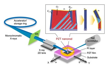
"We grew lead zirconate titanate films on different substrate types to induce different kinds of physical strain, and then selectively etched parts of the films to create nanorods," says lead author Tomoaki Yamada. "The domain structure of the nanorods was almost completely flipped compared with [that of] the thin film."
Lead zirconate titanate is a common type of ferroelectric material, which switches based on the movement of trapped lead atoms between two stable positions in the crystal lattice. Parts of the film were deliberately removed to leave freestanding rods on the substrates. The team then used synchrotron X-ray radiation to probe the domain structure of individual rods.
The contact area of the rods with the substrate was greatly reduced and the domain properties were influenced more by the surrounding environment, which mixed up the domain structure. The team found that coating the rods with a metal could screen the effects of the air and they tended to recover the original domain structure, as determined by the substrate.
"There are few effective ways of manipulating the domain structure of ferroelectric materials, and this becomes more difficult when the material is nanostructured and the contact area with the substrate is small." says collaborator Nava Setter. "We have learned that it's possible to nanostructure these materials with control over their domains, which is an essential step towards the new functional nanoscale devices promised by these materials."
Share on:


Suggested Items
Groundbreaking Ceremony Marks the Beginning of a New Era for Newccess Industrial; The Construction of the MINGXIN Building
04/12/2024 | Newccess IndustrialOn a clear and sunny day in March, the groundbreaking ceremony for the MINGXIN Building took place in Shenzhen, China. This moment marked the official commencement of construction for a project that will reshape the semiconductor materials industry.
The Need for a Holistic Global Sustainability Standard
04/10/2024 | Michael Ford, Aegis SoftwareNo one can deny that the resources of our fragile planet are finite. The environment seems like a third party, subject to constant degradation. We’re acutely aware of the effects of pollution on our climate, and despite our “throw-away” culture, recycling and recovery of materials has remained relatively expensive, even as we use more energy just to survive.
iNEMI Publishes Four Roadmap Topics
04/04/2024 | iNEMIThe International Electronics Manufacturing Initiative (iNEMI) announces the availability of the first roadmap topics in the new iNEMI Roadmap format. Printed circuit boards, sustainable electronics, smart manufacturing, and mmWave materials and test are now available online.
Insulectro’s 'Storekeepers' Extend Their Welcome to Technology Village at IPC APEX EXPO
04/03/2024 | InsulectroInsulectro, the largest distributor of materials for use in the manufacture of PCBs and printed electronics, welcomes attendees to its TECHNOLOGY VILLAGE during this year’s IPC APEX EXPO at the Anaheim Convention Center, April 9-11, 2024.
Checking In With ICAPE Group
04/03/2024 | Nolan Johnson, I-Connect007ICAPE Group’s field application engineer Erik Pederson drills down on sustainability, supply chain resiliency, and what value engineering really looks like in this exclusive interview. Founded in 1999, European-based ICAPE Group provides 21 million printed circuit boards and over six million technical parts to manufacturers every month. With 30 PCB manufacturing partners globally and 50 partners providing a wide array of technical parts, ICAPE Group has operations in China, Taiwan, Thailand, South Korea, Vietnam, South Africa, Europe, Mexico, and the United States. The company also focuses on the value proposition for its customers.