


 It’s Only Common Sense: OCCAM—the Time Is Now
 Marcy's Musings: The Growing Industry
 Dan’s Biz Bookshelf: Seeing the How
FAU-based Researchers Solve an Enigma of Solid State Physics
September 5, 2017 | FAUEstimated reading time: 2 minutes
Researchers at FAU and the Max Planck Institute (MPI) in Halle have managed to find the answer to one of the riddles of solid-state physics.
One of the fundamental phenomena of quantum physics is the fact that electrons appear to be able to tunnel through barriers that, to all intents and purposes, should be impenetrable. However this effect, which makes use of the wave-like nature of matter, is operative over very short distances only – for instance less than a nanometre in terms of individual atoms observed under a scanning tunnelling microscope – because of the exponential decay of the wave function within the barrier.
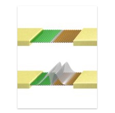
Thus, it was all the more surprising when, some ten years ago, it was discovered that an electrical current would flow for distances up to a thousand times longer in single and double layers of graphene – in other words, a layer of graphite with a thickness of one or two atoms – actually because of this exponential decay of wave functions. This new mechanism of electron transport, however, was difficult to analyse because it was barely distinguishable from the normal transport of electrons in a standard conductor.
Initially, it seemed the effect had been clearly understood, but it soon turned out to be much more complicated when a number of sensational experiments showed that seemingly identical double layer samples proved to be either very conductive or, quite the opposite, had a high level of resistivity. Solid-state physics was facing a puzzle. A number of well-received papers proposed that there must be exotic undiscovered new states of matter, although the theories were based on the resistivity observed only.
Theory of electron transport in defective double layers
While world-wide research in the field focused on explaining the phenomena on the assumption that the material itself was perfect, FAU-based researchers Dr. Sam Shallcross and Prof. Heiko B. Weber in cooperation with Dr. Sangeeta Sharma of MPI in Halle decided to go down a different route. They developed a theory whereby electron transport was occurring because of defects in these double layers, particularly because of stacking errors that can be compared to the creases in a two-layered table cloth.
Partial dislocations of this nature in graphene double-layers were discovered and analysed a few years ago at FAU. A new method of calculating the electronic structure in double layers, the first that was capable taking precisely these stacking errors into consideration, was developed for the theory. When this method is applied to a double layer of graphene, a new kind of electron transport can be posited that has a mathematical form like that of tunnelling but which is based on a qualitative new concept in physics – the assumption that, under certain circumstances, current can flow more efficiently if there are obstacles in the way.
Shallcross, Sharma and Weber discovered much to their own amazement that, depending on positioning, this electronic structure can behave either as a conductor or an insulator, hence explaining the perplexing results of the previous experiments. They have thus produced a comprehensive explanation of the entire phenomenology of graphene double layers with no need to postulate the existence of exotic new states.
This theoretical concept can be applied to many examples of an entire material class, namely the new and exciting two-dimensional materials. Their findings also serve to point out the fundamental differences in charge transport in our familiar three-dimensional world and the world of two-dimensional materials.
Share on:


Suggested Items
KIC’s Miles Moreau to Present Profiling Basics and Best Practices at SMTA Wisconsin Chapter PCBA Profile Workshop
01/25/2024 | KICKIC, a renowned pioneer in thermal process and temperature measurement solutions for electronics manufacturing, announces that Miles Moreau, General Manager, will be a featured speaker at the SMTA Wisconsin Chapter In-Person PCBA Profile Workshop.
The Drive Toward UHDI and Substrates
09/20/2023 | I-Connect007 Editorial TeamPanasonic’s Darren Hitchcock spoke with the I-Connect007 Editorial Team on the complexities of moving toward ultra HDI manufacturing. As we learn in this conversation, the number of shifting constraints relative to traditional PCB fabrication is quite large and can sometimes conflict with each other.
Standard Of Excellence: The Products of the Future
09/19/2023 | Anaya Vardya -- Column: Standard of ExcellenceIn my last column, I discussed cutting-edge innovations in printed circuit board technology, focusing on innovative trends in ultra HDI, embedded passives and components, green PCBs, and advanced substrate materials. This month, I’m following up with the products these new PCB technologies are destined for. Why do we need all these new technologies?
Experience ViTrox's State-of-the-Art Offerings at SMTA Guadalajara 2023 Presented by Sales Channel Partner—SMTo Engineering
09/18/2023 | ViTroxViTrox, which aims to be the world’s most trusted technology company, is excited to announce that our trusted Sales Channel Partner (SCP) in Mexico, SMTo Engineering, S.A. de C.V., will be participating in SMTA Guadalajara Expo & Tech Forum. They will be exhibiting in Booth #911 from the 25th to the 26th of October 2023, at the Expo Guadalajara in Jalisco, Mexico.
Intel Unveils Industry-Leading Glass Substrates to Meet Demand for More Powerful Compute
09/18/2023 | IntelIntel announced one of the industry’s first glass substrates for next-generation advanced packaging, planned for the latter part of this decade.