


 The Right Approach: I Hear the Train A Comin'
 It’s Only Common Sense: OCCAM—the Time Is Now
 Marcy's Musings: The Growing Industry
Newly Discovered Semiconductor Dynamics May Help Improve Energy Efficiency
September 6, 2017 | UICEstimated reading time: 2 minutes
Researchers examining the flow of electricity through semiconductors have uncovered another reason these materials seem to lose their ability to carry a charge as they become more densely “doped.”
Semiconductors are found in just about every piece of modern electronics, from computers to televisions to your cell phone. They fall somewhere between metals, which conduct electricity very well, and insulators like glass that don’t conduct electricity at all. This moderate conduction property is what allows semiconductors to perform as switches and transistors in electronics.
The most common material for semiconductors is silicon, which is mined from the earth and then refined and purified. But pure silicon doesn’t conduct electricity, so the material is purposely and precisely adulterated by the addition of other substances known as dopants. Boron and phosphorus ions are common dopants added to silicon-based semiconductors that allow them to conduct electricity.
But the amount of dopant added to a semiconductor matters – too little dopant and the semiconductor won’t be able to conduct electricity. Too much dopant and the semiconductor becomes more like a non-conductive insulator.
“There’s a sweet spot when it comes to doping where the right amount allows for the efficient conduction of electricity, but after a certain point, adding more dopants slows down the flow,” says Preston Snee, associate professor of chemistry at the University of Illinois at Chicago and corresponding author on the paper.
“For a long time scientists thought that the reason efficient conduction of electricity dropped off with the addition of more dopants was because these dopants caused the flowing electrons to be deflected away, but we found that there’s also another way too many dopants impede the flow of electricity.”
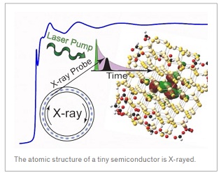
Snee, UIC chemistry student Asra Hassan, and their colleagues wanted to get a closer look at what happens when electricity flows through a semiconductor.
Using the Advanced Photon Source Argonne National Laboratory, they were able to capture X-ray images of what happens at the atomic level inside a semiconductor. They used tiny chips of cadmium sulfide for their semiconductor “base” and doped them with copper ions. Instead of wiring the tiny chips for electricity, they generated a flow of electrons through the semiconductors by shooting them with a powerful blue laser beam. At the same time, they took very high energy X-ray photos of the semiconductors at millionths of a microsecond apart – which showed what was happening at the atomic level in real time as electrons flowed through the doped semiconductors.
They found that when electrons were flowing through, the copper ions transiently formed bonds with the cadmium sulfate semiconductor base, which is detrimental to conduction.
“This has never been seen before,” said Hassan. “Electrons are still bouncing off dopants, which we knew already, but we now know of this other process that contributes to impeding flow of electricity in over-doped semiconductors.”
The bonding of the dopant ions to the semiconductor base material “causes the current to get stuck at the dopants, which we don’t want in our electronics, especially if we want them to be fast and efficient,” she said. “However, now that we know this is happening inside the material, we can design smarter systems that minimize this effect, which we call ‘charge carrier modulation of dopant bonding’.”
Xiaohan Liu, Ali Jawaid, Ahmet Gulec, Robert Klie and Armen Shamirian of UIC; Xiaoyi Zhang, Soma Chattopadhyay, Xiaobing Zuo of Argonne National Laboratory and Clare Rowland and Richard Schaller of Northwestern University are co-authors on the paper.
Share on:


Suggested Items
Designer’s Notebook: What Designers Need to Know About Manufacturing, Part 2
04/24/2024 | Vern Solberg -- Column: Designer's NotebookThe printed circuit board (PCB) is the primary base element for providing the interconnect platform for mounting and electrically joining electronic components. When assessing PCB design complexity, first consider the component area and board area ratio. If the surface area for the component interface is restricted, it may justify adopting multilayer or multilayer sequential buildup (SBU) PCB fabrication to enable a more efficient sub-surface circuit interconnect.
Insulectro’s 'Storekeepers' Extend Their Welcome to Technology Village at IPC APEX EXPO
04/03/2024 | InsulectroInsulectro, the largest distributor of materials for use in the manufacture of PCBs and printed electronics, welcomes attendees to its TECHNOLOGY VILLAGE during this year’s IPC APEX EXPO at the Anaheim Convention Center, April 9-11, 2024.
ENNOVI Introduces a New Flexible Circuit Production Process for Low Voltage Connectivity in EV Battery Cell Contacting Systems
04/03/2024 | PRNewswireENNOVI, a mobility electrification solutions partner, introduces a more advanced and sustainable way of producing flexible circuits for low voltage signals in electric vehicle (EV) battery cell contacting systems.
Heavy Copper PCBs: Bridging the Gap Between Design and Fabrication, Part 1
04/01/2024 | Yash Sutariya, Saturn Electronics ServicesThey call me Sparky. This is due to my talent for getting shocked by a variety of voltages and because I cannot seem to keep my hands out of power control cabinets. While I do not have the time to throw the knife switch to the off position, that doesn’t stop me from sticking screwdrivers into the fuse boxes. In all honesty, I’m lucky to be alive. Fortunately, I also have a talent for building high-voltage heavy copper circuit boards. Since this is where I spend most of my time, I can guide you through some potential design for manufacturability (DFM) hazards you may encounter with heavy copper design.
Trouble in Your Tank: Supporting IC Substrates and Advanced Packaging, Part 5
03/19/2024 | Michael Carano -- Column: Trouble in Your TankDirect metallization systems based on conductive graphite or carbon dispersion are quickly gaining acceptance worldwide. Indeed, the environmental and productivity gains one can achieve with these processes are outstanding. In today’s highly competitive and litigious environment, direct metallization reduces costs associated with compliance, waste treatment, and legal issues related to chemical exposure. What makes these processes leaders in the direct metallization space?