


 The Right Approach: I Hear the Train A Comin'
 It’s Only Common Sense: OCCAM—the Time Is Now
 Marcy's Musings: The Growing Industry
Semiconductor Patterning of Seven Nanometers Technology Using a Camera Flash
September 20, 2017 | KAISTEstimated reading time: 2 minutes
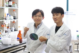
A research team led by Professor Sang Ouk Kim in the Department of Materials Science and Engineering at KAIST has developed semiconductor manufacturing technology using a camera flash.
This technology can manufacture ultra-fine patterns over a large area by irradiating a single flash with a seven-nanometer patterning technique for semiconductors. It can facilitate the manufacturing of highly efficient, integrated semiconductor devices in the future.
Technology for the Artificial Intelligence (AI), the Internet of Things (IoTs), and big data, which are the major keys for the fourth Industrial Revolution, require high-capacity, high-performance semiconductor devices. It is necessary to develop lithography technology to produce such next-generation, highly integrated semiconductor devices.
20170918143400_25291_1504586573.jpg
Although related industries have been using conventional photolithography for small patterns, this technique has limitations for forming a pattern of sub-10 nm patterns.
Molecular assembly patterning technology using polymers has been in the spotlight as the next generation technology to replace photolithography because it is inexpensive to produce and can easily form sub-10 nm patterns. However, since it generally takes a long time for heat treatment at high-temperature or toxic solvent vapor treatment, mass production is difficult and thus its commercialization has been limited.
The research team introduced a camera flash that instantly emits strong light to solve the issues of polymer molecular assembly patterning. Using a flash can possibly achieve a semiconductor patterning of seven nanometers within 15 milliseconds (1 millisecond = 1/1,000 second), which can generate a temperature of several hundred degrees Celsius in several tens of milliseconds.
The team has demonstrated that applying this technology to polymer molecular assembly allows a single flash of light to form molecular assembly patterns.
Formation of semiconductor patterns using a camera flash)
The team also identified its compatibility with polymer flexible substrates, which are impossible to process at high temperatures. Through these findings, the technology can be applied to the fabrication of next-generation, flexible semiconductors.
The researchers said the camera flash photo-thermal process will be introduced into molecular assembly technology and this highly-efficiency technology can accelerate the realization of molecular assembly semiconductor technology.
Schematic diagram of molecular assembly pattern using a camera flash
Professor Kim, who led the research, said, “Despite its potential, molecular assembly semiconductor technology has remained a big challenge in improving process efficiency.” “This technology will be a breakthrough for the practical use of molecular assembly-based semiconductors.”
The paper was published in the international journal, Advanced Materials on August 21 with first authors, researcher Hyeong Min Jin and PhD candidate Dae Yong Park.
The research, sponsored by the Ministry of Science and ICT, was co-led Professor by Keon Jae Lee in the Department of Materials Science and Engineering at KAIST, and Professor Kwang Ho Kim in the School of Materials Science and Engineering at Pusan National University.
Share on:


Suggested Items
Warm Windows and Streamlined Skin Patches – IDTechEx Explores Flexible and Printed Electronics
04/26/2024 | IDTechExFlexible and printed electronics can be integrated into cars and homes to create modern aesthetics that are beneficial and easy to use. From luminous car controls to food labels that communicate the quality of food, the uses of this technology are endless and can upgrade many areas of everyday life.
iNEMI Packaging Tech Topic Series: Role of EDA in Advanced Semiconductor Packaging
04/26/2024 | iNEMIAdvanced semiconductor packaging with heterogenous integration has made on-package integration of multiple chips a crucial part of finding alternatives to transistor scaling. Historically, EDA tools for front-end and back-end design have evolved separately; however, design complexity and the increased number of die-to-die or die-to-substrate interconnections has led to the need for EDA tools that can support integration of overall design planning, implementation, and system analysis in a single cockpit.
Koh Young Showcases Award-winning Inspection Solutions at SMTconnect with SmartRep in Hall 4A.225
04/25/2024 | Koh Young TechnologyKoh Young Technology, the industry leader in True 3D measurement-based inspection solutions, will showcase an array of award-winning inspection and measurement solutions at SMTconnect alongside its sales partner, SmartRep, in booth 4A.225 at NürnbergMesse from June 11-13, 2023. The following offers a glimpse into what Koh Young will present at the tradeshow:
Real Time with… IPC APEX EXPO 2024: Plasmatreat: Innovative Surface Preparation Solutions
04/25/2024 | Real Time with...IPC APEX EXPOIn this interview, Editor Nolan Johnson speaks with Hardev Grewal, CEO and president of Plasmatreat, a developer of atmospheric plasma solutions. Plasmatreat uses clean compressed air and electricity to create plasma, offering environmentally friendly methods for surface preparation. Their technology measures plasma density for process optimization and can remove organic micro-contamination. Nolan and Hardev also discuss REDOX-Tool, a new technology for removing metal oxides.
Nanotechnology Market to Surpass $53.51 Billion by 2031
04/25/2024 | PRNewswireSkyQuest projects that the nanotechnology market will attain a value of USD 53.51 billion by 2031, with a CAGR of 36.4% over the forecast period (2024-2031).