


 It’s Only Common Sense: OCCAM—the Time Is Now
 Marcy's Musings: The Growing Industry
 Dan’s Biz Bookshelf: Seeing the How
Scientists Make Atoms-Thick Post-It Notes for Solar Cells and Circuits
September 21, 2017 | University of ChicagoEstimated reading time: 2 minutes
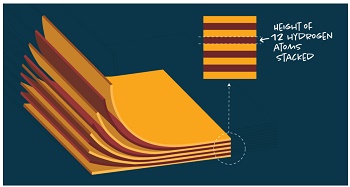
Over the past half-century, scientists have shaved silicon films down to just a wisp of atoms in pursuit of smaller, faster electronics. For the next set of breakthroughs, though, they’ll need novel ways to build even tinier and more powerful devices.
In a study published Sept. 20 in Nature, University of Chicago and Cornell University researchers describe an innovative method to make stacks of semiconductors just a few atoms thick. The technique offers scientists and engineers a simple, cost-effective method to make thin, uniform layers of these materials, which could expand capabilities for devices from solar cells to cell phones.
Stacking thin layers of materials offers a range of possibilities for making electronic devices with unique properties. But manufacturing such films is a delicate process, with little room for error.
“The scale of the problem we’re looking at is, imagine trying to lay down a flat sheet of plastic wrap the size of Chicago without getting any air bubbles in it,” said Jiwoong Park, a UChicago professor in the Department of Chemistry, the Institute for Molecular Engineering and the James Franck Institute, who led the study. “When the material itself is just atoms thick, every little stray atom is a problem.”
Today, these layers are “grown” instead of stacking them on top of one another. But that means the bottom layers have to be subjected to harsh growth conditions such as high temperatures while the new ones are added—a process that limits the materials with which to make them.
Park’s team instead made the films individually. Then they put them into a vacuum, peeled them off and stuck them to one another, like Post-It notes. This allowed the scientists to make films that were connected with weak bonds instead of stronger covalent bonds—interfering less with the perfect surfaces between the layers.
“The films, vertically controlled at the atomic-level, are exceptionally high-quality over entire wafers,” said Kibum Kang, a postdoctoral associate who was the first author of the study.
Kan-Heng Lee, a graduate student and co-first author of the study, then tested the films’ electrical properties by making them into devices and showed that their functions can be designed on the atomic scale, which could allow them to serve as the essential ingredient for future computer chips.
The method opens up a myriad of possibilities for such films. They can be made on top of water or plastics; they can be made to detach by dipping them into water; and they can be carved or patterned with an ion beam. Researchers are exploring the full range of what can be done with the method, which they said is simple and cost-effective.
“We expect this new method to accelerate the discovery of novel materials, as well as enabling large-scale manufacturing,” Park said.
Share on:


Suggested Items
SMC Korea 2024 to Highlight Semiconductor Materials Trends and Innovations on Industry’s Path to $1 Trillion
04/24/2024 | SEMIWith Korea a major consumer of semiconductor materials and advanced materials a key driver of innovation on the industry’s path to $1 trillion, industry leaders and experts will gather at SMC (Strategic Materials Conference) Korea 2024 on May 29 at the Suwon Convention Center in Gyeonggi-do, South Korea to provide insights into the latest materials developments and trends. Registration is open.
Groundbreaking Ceremony Marks the Beginning of a New Era for Newccess Industrial; The Construction of the MINGXIN Building
04/12/2024 | Newccess IndustrialOn a clear and sunny day in March, the groundbreaking ceremony for the MINGXIN Building took place in Shenzhen, China. This moment marked the official commencement of construction for a project that will reshape the semiconductor materials industry.
The Need for a Holistic Global Sustainability Standard
04/10/2024 | Michael Ford, Aegis SoftwareNo one can deny that the resources of our fragile planet are finite. The environment seems like a third party, subject to constant degradation. We’re acutely aware of the effects of pollution on our climate, and despite our “throw-away” culture, recycling and recovery of materials has remained relatively expensive, even as we use more energy just to survive.
iNEMI Publishes Four Roadmap Topics
04/04/2024 | iNEMIThe International Electronics Manufacturing Initiative (iNEMI) announces the availability of the first roadmap topics in the new iNEMI Roadmap format. Printed circuit boards, sustainable electronics, smart manufacturing, and mmWave materials and test are now available online.
Insulectro’s 'Storekeepers' Extend Their Welcome to Technology Village at IPC APEX EXPO
04/03/2024 | InsulectroInsulectro, the largest distributor of materials for use in the manufacture of PCBs and printed electronics, welcomes attendees to its TECHNOLOGY VILLAGE during this year’s IPC APEX EXPO at the Anaheim Convention Center, April 9-11, 2024.