


 It’s Only Common Sense: OCCAM—the Time Is Now
 Marcy's Musings: The Growing Industry
 Dan’s Biz Bookshelf: Seeing the How
Advanced Molybdenum Selenide Near Infrared Phototransistors
September 29, 2017 | University of Electro-CommunicationsEstimated reading time: 1 minute
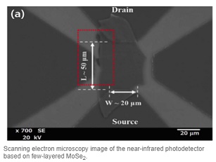
Optical sensors operating in the near infrared (NIR) are important for applications in imaging, photodetectors, and biological sensors. Notably, recent reports on the synthesis of high quality, large areas of graphene has motivated researchers to search for other 2D materials with properties suitable for NIR devices.
Now, Abdelkader Abderrahmane and colleagues at the University of Electro-Communications, Tokyo in collaboration with researchers at Chosun University, Korea, describe the optoelectronics characteristics of molybdenum selenide (MoSe2) phototransistors for applications to photodetectors. The application of gate voltages to the devices yielded a maximum photoresponsivity 238 A/W, an external quantum efficiency (EQE) of 37,745% under 785 nm light. The researchers state: "our device is one of the best high-performance nanoscale near-infrared photodetectors based on multilayered two-dimensional materials."
The devices were fabricated using few layered MoSe2 with a thickness of ~44 nm that was exfoliated from natural MoSe2 onto thermally oxidized silicon substrates with metallic strips acting as back gates. The transistor channel width and length were 50 and 20 μm, and the charge mobility was be 5.1 cm2 /V/s.
Electrical measurements indicated that the devices operated in the so-called accumulation mode and with a pinch off voltage of - 40V.
The combination of the 1.1 eV bandgap of MoSe2 and its high optical absorption compared to MoS2 is expected to offer wide ranging applications in optoelectronics.
Share on:


Suggested Items
Inkjet Solder Mask ‘Has Arrived’
04/10/2024 | Pete Starkey, I-Connect007I was delighted to be invited to attend an interactive webinar entitled “Solder Mask Coating Made Easy with Additive Manufacturing,” hosted by SUSS MicroTec Netherlands in Eindhoven. The webinar was introduced and moderated by André Bodegom, managing director at Adeon Technologies, and the speakers were Mariana Van Dam, senior product manager PCB imaging solutions at AGFA in Belgium; Ashley Steers, sales manager at Electra Polymers in the UK; and Dr. Luca Gautero, product manager at SUSS MicroTec Netherlands.
NetVia Group Acquires Direct Imaging from Mivatek
04/09/2024 | Miva TechnologiesMiva Technologies is pleased to announce NetVia Group, Irving, TX has acquired a new Miva 2400NG Dual Tray Direct Imaging System with 30-micron capabilities for inner, outer and soldermask imaging.
Teledyne to Acquire Adimec
02/13/2024 | TeledyneTeledyne Technologies Incorporated announced that it has entered into an agreement to acquire Adimec Holding B.V. and its subsidiaries.
Real Time with... productronica 2023: MivaTek Global Advances Technology With High-res Imaging System
12/08/2023 | Real Time with...productronicaMivaTek's Brendan Hogan talks about how the company employs Digitally Adaptive Rasterization Technology (DART) in their high-res imaging equipment. He also shares how the blurred line between semiconductors and microelectronics is driving broader application of the imaging process.
Keysight Enables Validation of Arbe 4D Imaging Radar Chipset
11/30/2023 | Keysight Technologies, Inc.Keysight Technologies, Inc. announces that Arbe has selected the E8719A Radar Target Solution (RTS) to test the Arbe 4D imaging radar chipset for automotive applications.