


 Happy’s Tech Talk #28: The Power Mesh Architecture for PCBs
 It’s Only Common Sense: Would You Join Your Own Company?
 The Chemical Connection: Reducing Etch System Water Usage, Part 2
Atotech Presents a Novel E’Less Copper and Blackening Process for Touchscreen Application at the Eurodisplay 2017
November 1, 2017 | AtotechEstimated reading time: 2 minutes
Atotech is one of the world’s leading manufacturers of specialty chemicals and equipment for the printed circuit board, IC-substrate and semiconductor industries, as well as for the decorative and functional surface finishing industries. As touchscreens become higher in demand and traditional build-up technology based on vapor deposited Indium Tin Oxide (ITO) reach its limitations, the new metal mesh technology to produce the sensor grid for advanced touch screens and sensors finds its momentum. While ITO has a low conductivity and is a brittle material, copper meshes feature a low resistance – ideal for use in large displays – coupled with the mechanical properties required for flexible or curved touch screens.
Visitors to the Eurodisplay 2017 are invited to learn more about this novel, additive and ITO free process for the formation of metal mesh and TFT electrodes.
When: Thursday, November 2, at 3:40pm
Where: Berlin, Melia Hotel, Friedrichstraße 103
Presenter: Roger Massey, Business Development Manager at Atotech GmbH
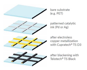
Cupratech TS D3 and Telotech® TS Black – Solutions for fully additive processing of Cu mesh touch sensors
Cupratech TS D3
Atotech’s metallization specialists have developed a new and tailor-made electroless copper process which allows the full additive build-up of copper meshes based on catalytic palladium or silver layers. “Cupratech® TS D3 features quick initiation and a high deposition rate of up to 140 nm/min for a minimized attack on the conductor tracks,” states Lars-Eric Pribyl, Global Product Manager Desmear and Metallization at Atotech Deutschland GmbH. “The process deposits a fine grain copper layer with high conductivity over the entire sensor. It is mass production proven and has been optimized to enable an excellent track shape.”
Telotech TS Black
Touch sensors are used in applications where the user does not want to see the conductor tracks within their display. “With Telotech TS Black, Atotech has developed a unique blackening process that greatly reduces the visibility of copper conductors on transparent substrates like PET,” continues Pribyl. “The process features very mild process conditions and provides a uniform black/dark finish to copper structures and surfaces. Like Cupratech TS D3, Telotech TS Black is applied in horizontal or reel-to-reel manufacturing equipment.”
Eurodisplay will be held from October 31 to November 2, 2017, in Berlin, Germany and discusses the latest development in all types of displays, electronics, and their impact on society.
About Atotech
Atotech is one of the world’s leading manufacturers of specialty chemicals and equipment for the printed circuit board, IC-substrate and semiconductor industries, as well as for the decorative and functional surface finishing industries. Atotech has annual sales of USD1.1 billion. The company is fully committed to sustainability – we develop technologies to minimize waste and to reduce environmental impact. Atotech has its headquarters in Berlin, Germany, and employs more than 4,000 people in over 40 countries.
Share on:


Suggested Items
The Chemical Connection: Reducing Etch System Water Usage, Part 2
05/02/2024 | Don Ball -- Column: The Chemical ConnectionIn my last column, I reviewed some relatively simple ways to reduce water usage in existing etch systems: cutting down cooling coil water flow, adding chillers to replace plant water for cooling, lowering flow rate nozzles for rinses, etc. This month, I’ll continue with more ways to control water usage in your etcher. Most of these are not easily retrofittable to existing equipment but should be given serious consideration when new equipment is contemplated. With the right combination of add-ons, it is possible to bring the amount of water used in an etch system to almost zero.
Designer’s Notebook: What Designers Need to Know About Manufacturing, Part 2
04/24/2024 | Vern Solberg -- Column: Designer's NotebookThe printed circuit board (PCB) is the primary base element for providing the interconnect platform for mounting and electrically joining electronic components. When assessing PCB design complexity, first consider the component area and board area ratio. If the surface area for the component interface is restricted, it may justify adopting multilayer or multilayer sequential buildup (SBU) PCB fabrication to enable a more efficient sub-surface circuit interconnect.
Insulectro’s 'Storekeepers' Extend Their Welcome to Technology Village at IPC APEX EXPO
04/03/2024 | InsulectroInsulectro, the largest distributor of materials for use in the manufacture of PCBs and printed electronics, welcomes attendees to its TECHNOLOGY VILLAGE during this year’s IPC APEX EXPO at the Anaheim Convention Center, April 9-11, 2024.
ENNOVI Introduces a New Flexible Circuit Production Process for Low Voltage Connectivity in EV Battery Cell Contacting Systems
04/03/2024 | PRNewswireENNOVI, a mobility electrification solutions partner, introduces a more advanced and sustainable way of producing flexible circuits for low voltage signals in electric vehicle (EV) battery cell contacting systems.
Heavy Copper PCBs: Bridging the Gap Between Design and Fabrication, Part 1
04/01/2024 | Yash Sutariya, Saturn Electronics ServicesThey call me Sparky. This is due to my talent for getting shocked by a variety of voltages and because I cannot seem to keep my hands out of power control cabinets. While I do not have the time to throw the knife switch to the off position, that doesn’t stop me from sticking screwdrivers into the fuse boxes. In all honesty, I’m lucky to be alive. Fortunately, I also have a talent for building high-voltage heavy copper circuit boards. Since this is where I spend most of my time, I can guide you through some potential design for manufacturability (DFM) hazards you may encounter with heavy copper design.