


 It’s Only Common Sense: OCCAM—the Time Is Now
 Marcy's Musings: The Growing Industry
 Dan’s Biz Bookshelf: Seeing the How
Folding Circuits Just Atoms Thick Using the Principles of Origami
November 2, 2017 | AVS: Science and Technology of Materials, Interfaces, and ProcessingEstimated reading time: 2 minutes
While the creation of a paper swan using origami may be intriguing, the idea of creating 3-D circuits based on similar design principles is simply mindboggling. Researchers have focused on large scale synthesis and device fabrication using ultra-thin materials, which has led to improvements in 2-D models and the introduction of 3-D vertically integrated devices.
A new method allows scientists to craft individual tiny films, each just a few atoms high, and stack them for new kinds of electronics. Credit: Luis Ibarra, University of Chicago Creative
Origami, the well-known Japanese art of paper folding, generates complex 3-D structures from flat 2-D paper. While the creation of a paper swan may be intriguing, the idea of creating 3-D circuits based on similar design principles is simply mindboggling. This science fiction-sounding research is a project that Jiwoong Park and colleagues from the University of Chicago have been developing over the last few years.
Park's focus on large scale synthesis and device fabrication using ultra-thin materials has led to improvements in 2-D models and the introduction of 3-D vertically integrated devices.
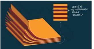
Using atomically thin materials, Park synthesizes large scale integrated circuits that can be stitched together laterally to form a 2-D module. In their most recent project, his team has vertically integrated these 2-D modules to produce 3-D stacks.
Circuits have traditionally been developed using bulky substrate platforms, like silicon, and until recently were unable to function independently. Circuits based only on atomically thin materials liberate research from these conventional limitations. Combining various ultra-thin building blocks also allows for the integration of different electric and thermal properties within the same circuit, exponentially increasing functionality.
"For our research, we first generate atomically thin paper with different color[s] representing different electrical, optical, or thermal properties. We combine them in the lateral direction, equivalent to stitching. We stack them on top of one another, which is vertical integration. By doing so we are trying to develop large scale, fully functioning integrated circuits using these atomically thin materials as 2-D building blocks or color paper," Park said.
The use of these ultra-thin materials, as opposed to typical components and resources, allows for a smaller circuit, but surprisingly not one that is microscopically small and therefore difficult to manipulate. The 2-D ingredients are assembled in such a way that they can be viewed with a simple optical microscope or even with the naked eye and can be handled accordingly.
Potential applications of this technology are also extensive. Similar to the way folding is applicable in objects used in day-to-day life, such as umbrellas or parachutes, integrated circuits would be able to contain a large surface area in a relatively condensed volume. Functionality in this context could be applied to a diverse set of new devices using the capabilities of condensed circuitry.
"What we are interested in developing is this mechanism of taking all these surfaces and device elements and folding them into tight spaces. Upon our cue, we want them to deploy to really large functioning surfaces," Park said.
Share on:


Suggested Items
SMC Korea 2024 to Highlight Semiconductor Materials Trends and Innovations on Industry’s Path to $1 Trillion
04/24/2024 | SEMIWith Korea a major consumer of semiconductor materials and advanced materials a key driver of innovation on the industry’s path to $1 trillion, industry leaders and experts will gather at SMC (Strategic Materials Conference) Korea 2024 on May 29 at the Suwon Convention Center in Gyeonggi-do, South Korea to provide insights into the latest materials developments and trends. Registration is open.
Groundbreaking Ceremony Marks the Beginning of a New Era for Newccess Industrial; The Construction of the MINGXIN Building
04/12/2024 | Newccess IndustrialOn a clear and sunny day in March, the groundbreaking ceremony for the MINGXIN Building took place in Shenzhen, China. This moment marked the official commencement of construction for a project that will reshape the semiconductor materials industry.
The Need for a Holistic Global Sustainability Standard
04/10/2024 | Michael Ford, Aegis SoftwareNo one can deny that the resources of our fragile planet are finite. The environment seems like a third party, subject to constant degradation. We’re acutely aware of the effects of pollution on our climate, and despite our “throw-away” culture, recycling and recovery of materials has remained relatively expensive, even as we use more energy just to survive.
iNEMI Publishes Four Roadmap Topics
04/04/2024 | iNEMIThe International Electronics Manufacturing Initiative (iNEMI) announces the availability of the first roadmap topics in the new iNEMI Roadmap format. Printed circuit boards, sustainable electronics, smart manufacturing, and mmWave materials and test are now available online.
Insulectro’s 'Storekeepers' Extend Their Welcome to Technology Village at IPC APEX EXPO
04/03/2024 | InsulectroInsulectro, the largest distributor of materials for use in the manufacture of PCBs and printed electronics, welcomes attendees to its TECHNOLOGY VILLAGE during this year’s IPC APEX EXPO at the Anaheim Convention Center, April 9-11, 2024.