


 Happy’s Tech Talk #28: The Power Mesh Architecture for PCBs
 It’s Only Common Sense: Would You Join Your Own Company?
 The Chemical Connection: Reducing Etch System Water Usage, Part 2
Optoelectronics Without Glass
November 7, 2017 | ETH ZurichEstimated reading time: 3 minutes
Researchers at ETH Zurich have developed the first opto-electronic circuit component that works without glass and is instead made of metal. The component, referred to as a modulator, converts electrical data signals into optical signals. It is smaller and faster than current modulators, and much easier and cheaper to make.
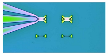
Microscopic image of a chip. Top left: functional modulator with electrical contacts; right: test modulator without electrical contact; below: test components. (Photograph: ETH Zurich)
Optical components for microelectronics must be made of glass. Metals are not suitable for this purpose, since optical data can propagate only across roughly a distance of 100 micrometres. This was the general view of scientists until recently. A team of researchers headed by Juerg Leuthold, professor in the Department of Information Technology and Electrical Engineering, has now succeeded in doing what was thought to be impossible and developed a light-processing component made of metal. The researchers have presented their findings in the latest issue of the journal Science.
They accomplished this feat by building a small enough component: at just 3 x 36 micrometres, it is within a size range in which both optical and electrical information can propagate in metals.
Component for fibre optic networks
The component is a modulator: modulators convert electrical data signals into optical signals. They are installed in modern internet routers used for fibre optic networks and enable fibre optic data connections between computer units in data centres. However, the standard components used today function differently than the new modulators.
The new component works by aiming the light from a fibre optic source at the modulator, causing the electrons on its surface to oscillate. Experts refer to this as a surface plasmon oscillation. This oscillation can be changed indirectly by electrical data pulses. When the oscillation of the electrons is converted back into light, the electrical information is now encoded onto the optical signal. This means that the information is converted from an electrical into an optical data pulse that can be transmitted via fibre optics.
Schematic representation of the metallic modulator: Left: a continuous beam of light strikes a metallic lattice that deflects the light onto the chip. Right: an optical data pulse exits the component. (Photograph: ETH Zurich)
Faster and smaller
Two years ago, Leuthold and his colleagues developed one of these plasmonic modulators (ETH News reported). At the time, it was the smallest and fastest modulator ever built, but the semiconductor chip still had various glass components.
By replacing all the glass components with metallic ones, the scientists have succeeded in building an even smaller modulator that works up to highest speed. “In metals, electrons can move at practically any speed, whereas the speed in glass is limited due to its physical properties,” says Masafumi Ayata, a doctoral student in Leuthold’s group and lead author of the study. In the experiment, the researchers succeeded in transmitting data at 116 gigabits per second. They are convinced that with further improvements, even higher data transfer rates will be possible.
Page 1 of 2
Share on:


Suggested Items
The Chemical Connection: Reducing Etch System Water Usage, Part 2
05/02/2024 | Don Ball -- Column: The Chemical ConnectionIn my last column, I reviewed some relatively simple ways to reduce water usage in existing etch systems: cutting down cooling coil water flow, adding chillers to replace plant water for cooling, lowering flow rate nozzles for rinses, etc. This month, I’ll continue with more ways to control water usage in your etcher. Most of these are not easily retrofittable to existing equipment but should be given serious consideration when new equipment is contemplated. With the right combination of add-ons, it is possible to bring the amount of water used in an etch system to almost zero.
Designer’s Notebook: What Designers Need to Know About Manufacturing, Part 2
04/24/2024 | Vern Solberg -- Column: Designer's NotebookThe printed circuit board (PCB) is the primary base element for providing the interconnect platform for mounting and electrically joining electronic components. When assessing PCB design complexity, first consider the component area and board area ratio. If the surface area for the component interface is restricted, it may justify adopting multilayer or multilayer sequential buildup (SBU) PCB fabrication to enable a more efficient sub-surface circuit interconnect.
Insulectro’s 'Storekeepers' Extend Their Welcome to Technology Village at IPC APEX EXPO
04/03/2024 | InsulectroInsulectro, the largest distributor of materials for use in the manufacture of PCBs and printed electronics, welcomes attendees to its TECHNOLOGY VILLAGE during this year’s IPC APEX EXPO at the Anaheim Convention Center, April 9-11, 2024.
ENNOVI Introduces a New Flexible Circuit Production Process for Low Voltage Connectivity in EV Battery Cell Contacting Systems
04/03/2024 | PRNewswireENNOVI, a mobility electrification solutions partner, introduces a more advanced and sustainable way of producing flexible circuits for low voltage signals in electric vehicle (EV) battery cell contacting systems.
Heavy Copper PCBs: Bridging the Gap Between Design and Fabrication, Part 1
04/01/2024 | Yash Sutariya, Saturn Electronics ServicesThey call me Sparky. This is due to my talent for getting shocked by a variety of voltages and because I cannot seem to keep my hands out of power control cabinets. While I do not have the time to throw the knife switch to the off position, that doesn’t stop me from sticking screwdrivers into the fuse boxes. In all honesty, I’m lucky to be alive. Fortunately, I also have a talent for building high-voltage heavy copper circuit boards. Since this is where I spend most of my time, I can guide you through some potential design for manufacturability (DFM) hazards you may encounter with heavy copper design.