


 The Right Approach: I Hear the Train A Comin'
 It’s Only Common Sense: OCCAM—the Time Is Now
 Marcy's Musings: The Growing Industry
New Insights on 'Captured' Electrons Could Improve Flash Memory
November 8, 2017 | NISTEstimated reading time: 4 minutes
An entirely new model of the way electrons are briefly trapped and released in tiny electronic devices suggests that a long-accepted, industry-wide view is just plain wrong about the way these captured electrons affect the behavior of hardware components such as flash memory cells.
The model, devised by scientists at the National Institute of Standards and Technology (NIST), was tested to explain how electron capture and emission creates the insidious noise that increasingly threatens performance as electronic devices continue to shrink in size.
Those effects, variously known as burst noise, popcorn noise or random telegraph noise (RTN) “have become a major problem for extremely small devices,” said NIST researcher Kin Cheung, the lead author of a new report (link is external) in IEEE Transactions on Electron Devices.
Charge trapping is one of the known causes of flash memory failure. The new model, which NIST physicist John Kramar called “a major paradigm shift in charge-trapping modeling,” could lead to a different approach to manage this problem, and potentially, a new way of making the memory cells smaller.
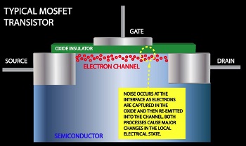
Typical MOSFET transistor
RTN noise consists of abrupt random drops in voltage or current caused by itinerant electrons that are briefly captured from, and then rejoin, the main flow along a current channel in, for example, a common type of transistor called a MOSFET.
“The effect was mostly negligible back in the good old days when devices were larger and there were lots of electrons flowing around,” Cheung said. But in today’s advanced devices, with feature dimensions in the range of 10 nanometers (nm, billionths of a meter) or less, the active area is so small that it can be swamped by a single trapped charge.
“As you get down to the very smallest sizes, RTN can be nearly 100 percent as strong as the signal you’re trying to measure,” Cheung said. “In those conditions, reliability disappears.”
In the case of RTN, the basics are known: The noise is caused by the action of electrons near the interface between two materials such as an insulator layer and the bulk of the semiconductor in a transistor. Specifically, an electron is pulled out of the current flow and trapped in a defect in the insulator; after a short time, it is emitted back into the main current in the semiconductor. What actually happens on the atomic scale at each stage of the process, however, is incompletely understood.
The orthodox approach to account for those effects is to treat all the trapped electrons as a single 2-D sheet of charge that extends uniformly across the center of the insulator. Each emitted electron is thought to return to the semiconductor in a reverse of the same process by which it was captured, causing very little change in the presumably stable state along the insulator/semiconductor boundary.
That model, when applied to very small devices, didn’t make sense to the NIST scientists. Among other difficulties, it ignored the fact that, once they are immobilized, electrons cause considerable distortions in local electrical field conditions along the boundary, affecting current flow. “We’re saying the traditional way doesn’t really work,” Cheung said. “You have to rethink this thing. The old model doesn’t make reasonable assumptions about how charge carriers behave.”
The researchers proposed a new model, based on local effects, in which the mechanisms of capture and emission are dramatically different from the standard picture. For one thing, they determined that quantum mechanics, the modern theory that describes the behavior of these systems, makes it hugely improbable, if not impossible, for electrons to get out of the insulator the same way they got in.
“It’s like a highway where there is an exit ramp, but there’s no on ramp,” says NIST co-author Jason Campbell. “You can go in, but you can’t come back that way. You’ve got to come back a different way. That is, there is a set of rules for capture that don’t apply to emission.”
“When you realize that the capture and emission processes are decoupled,” Cheung said, “you quickly have a very different view of the problem.”
The standard RTN picture supposes a weak interaction of trapped charge with its local surroundings―in this case, the highly separated electric charge in the silicon dioxide that often makes up the insulator layer in a transistor. NIST scientists found that a weak interaction is inconsistent with known physics and not in agreement with reports from two independent laboratories. Indeed, the interaction energy of a captured electron can be more than 10 times greater than previously believed. Recognition of this stronger interaction energy enables the new local field picture to explain RTN naturally.
The success of the new model, and the resulting drastic change in the understanding of both capture and emission, suggested that many long-held ideas would have to be thoroughly reconsidered.
“That was a very scary, very unsettling conclusion,” Campbell said. “I mean, this is tear-up-the-textbook stuff.”
The researchers hope the new model will help chip engineers and designers understand in much greater detail how devices degrade, and what will be required to get to the next stage of miniaturization while maintaining reliability and reducing noise.
Share on:


Suggested Items
Mycronic Releases Interim Report January–March 2024
04/18/2024 | MycronicNet sales increased 39 percent to SEK 1,692 (1,219) million. Based on constant exchange rates, net sales increased 42 percent.
NCAB Appoints Tim Benjamin as New CFO
04/15/2024 | NCAB GroupNCAB Group has appointed Tim Benjamin as its new CFO. Tim has a long and broad experience of managerial business finance roles, including M&A and IT.
TT Electronics Awarded Contract with Kongsberg Defence and Aerospace
04/11/2024 | TT ElectronicsTT Electronics, a leading provider of global manufacturing solutions and engineered technologies, announced today that its Fairford UK business has been awarded a new contract with long-standing customer Kongsberg Defence and Aerospace (Kongsberg) for the production of complex cable harness solutions.
IPC APEX EXPO 2024: There’s an App for That
04/03/2024 | Kim DiCianni, IPCWith so many things to do at a large trade show and conference like IPC APEX EXPO, you cannot possibly take every class, attend every talk, or see every vendor on your list. But you can plan your days and maximize your time with the IPC APEX EXPO mobile app. The app allows you to easily view the show’s daily agenda, keynote speakers, the conference and professional development schedules, and, of course, flag and make notes on exhibitors.
It’s Only Common Sense: When Your Company Starts Running Out of Popcorn
04/01/2024 | Dan Beaulieu -- Column: It's Only Common SenseCompanies, like people, get tired. I have seen companies just lose their focus, their “raison d’etre,” and just, well, fade away. More than once, I have sat in the office of a company owner, trying to console him while he asks me to “get him out of there.” Owners just get tired of the daily grind. They want off the treadmill of the constant juggling of people, strategies, customers, and, of course, cash flow.