


 Marcy's Musings: The Growing Industry
 It’s Only Common Sense: Here’s What To Do After IPC APEX EXPO 2024
 Dan’s Biz Bookshelf: Seeing the How
Strain-Free Epitaxy of Germanium Film on Mica
November 20, 2017 | AMERICAN INSTITUTE OF PHYSICSEstimated reading time: 2 minutes
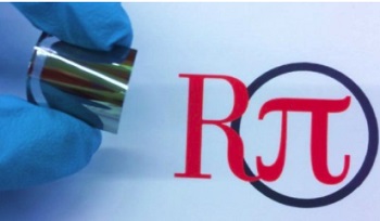
Germanium was the material of choice in the early history of electronic devices, and due to its high charge carrier mobility, it's making a comeback. It's generally grown on expensive single-crystal substrates, adding another challenge to making it sustainably viable for most applications. To address this aspect, researchers demonstrate an epitaxy method that incorporates van der Waals' forces to grow germanium on mica.
Germanium, an elemental semiconductor, was the material of choice in the early history of electronic devices, before it was largely replaced by silicon. But due to its high charge carrier mobility -- higher than silicon by threefold -- the semiconductor is making a comeback.
Germanium (Ge) is generally grown on expensive single-crystal substrates, adding another challenge to making it sustainably viable for most applications. To address this aspect, researchers at Rensselaer Polytechnic Institute in the United States demonstrate an epitaxy method that incorporates van der Waals' forces to grow Ge on mica. Applications could include advanced integrated circuits and high-efficiency solar cells.
"This is the first time strain-free van der Waals epitaxy of an elemental semiconductor has been demonstrated on mica," said Aaron Littlejohn, RPI researcher and co-author of the paper demonstrating the work, published recently in the Journal of Applied Physics, from AIP Publishing.
Growing crystalline film layers on crystalline substrates (called epitaxy) is ubiquitous in semiconductor fabrication. If the film and substrate materials are the same, then the perfectly matched layers form strong chemical bonds for optimal charge carrier mobility.
Layering different materials effectively, however, is a challenge because the crystal lattices typically don't align. To get around this, researchers employed vdW forces, phenomena that are based on the probabilistic nature of electrons, which are not in a fixed position around a nucleus. Rather, they can be anywhere, and the probability that they will be unevenly distributed exists almost all the time. When this happens, there is an induced dipole: a slight positive charge on one side and a slight negative charge opposite. This produces weakly attractive interactions between neutral atoms.
The researchers chose mica as the substrate on which to grow the Ge film because of its atomically smooth surface, which is free of dangling bonds (unpaired valence electrons). This ensured that no chemical bonding would take place during the vdW epitaxy process.
Instead, the materials' interface is held together via weak vdW forces. This allows for the growth of a relaxed film despite the dramatically different crystal structures of the two materials which have a 23 percent difference in atomic spacings. In addition to alleviating the constraints of lattice matching, vdW epitaxy allows the Ge film to be mechanically exfoliated from the mica surface and stand alone as a substrateless film.
"Our Ge film could be used as a thin-film nanomembrane, which could be integrated into electronic devices more easily than nanocrystals or nanowires," Littlejohn said. "It could also serve as the substrate for the subsequent deposition of additional materials for flexible transistors and solar cells, or even wearable optoelectronics."
Geranium films about 80 nanometers thick were grown on millimeter-scale muscovite mica substrates .26 mm thick. By varying the substrate temperature during deposition and annealing in the range of 300-500 degrees Celsius, the researchers found that the crystal lattice stabilizes at about 425 degrees Celsius.
"Previous research implies that elemental semiconductors cannot be epitaxially grown on mica using vdW forces at any elevated temperature, but we have now shown otherwise," Littlejohn said. "With the success of our Ge film grown on mica at a practical temperature, we anticipate that other nonlayered elemental or alloyed materials can be grown on mica via vdW epitaxy."
Share on:


Suggested Items
Groundbreaking Ceremony Marks the Beginning of a New Era for Newccess Industrial; The Construction of the MINGXIN Building
04/12/2024 | Newccess IndustrialOn a clear and sunny day in March, the groundbreaking ceremony for the MINGXIN Building took place in Shenzhen, China. This moment marked the official commencement of construction for a project that will reshape the semiconductor materials industry.
The Need for a Holistic Global Sustainability Standard
04/10/2024 | Michael Ford, Aegis SoftwareNo one can deny that the resources of our fragile planet are finite. The environment seems like a third party, subject to constant degradation. We’re acutely aware of the effects of pollution on our climate, and despite our “throw-away” culture, recycling and recovery of materials has remained relatively expensive, even as we use more energy just to survive.
iNEMI Publishes Four Roadmap Topics
04/04/2024 | iNEMIThe International Electronics Manufacturing Initiative (iNEMI) announces the availability of the first roadmap topics in the new iNEMI Roadmap format. Printed circuit boards, sustainable electronics, smart manufacturing, and mmWave materials and test are now available online.
Insulectro’s 'Storekeepers' Extend Their Welcome to Technology Village at IPC APEX EXPO
04/03/2024 | InsulectroInsulectro, the largest distributor of materials for use in the manufacture of PCBs and printed electronics, welcomes attendees to its TECHNOLOGY VILLAGE during this year’s IPC APEX EXPO at the Anaheim Convention Center, April 9-11, 2024.
Checking In With ICAPE Group
04/03/2024 | Nolan Johnson, I-Connect007ICAPE Group’s field application engineer Erik Pederson drills down on sustainability, supply chain resiliency, and what value engineering really looks like in this exclusive interview. Founded in 1999, European-based ICAPE Group provides 21 million printed circuit boards and over six million technical parts to manufacturers every month. With 30 PCB manufacturing partners globally and 50 partners providing a wide array of technical parts, ICAPE Group has operations in China, Taiwan, Thailand, South Korea, Vietnam, South Africa, Europe, Mexico, and the United States. The company also focuses on the value proposition for its customers.