


 Marcy's Musings: The Growing Industry
 It’s Only Common Sense: Here’s What To Do After IPC APEX EXPO 2024
 Dan’s Biz Bookshelf: Seeing the How
The Stacked Color Sensor
November 27, 2017 | EMPAEstimated reading time: 3 minutes
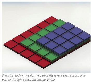
Red-sensitive, blue-sensitive and green-sensitive color sensors stacked on top of each other instead of being lined up in a mosaic pattern – this principle could allow image sensors with unprecedented resolution and sensitivity to light to be created. However, so far, the reality hasn't quite met expectations. Researchers from Empa and ETH Zurich have now developed a sensor prototype that absorbs light almost optimally – and is also cheap to produce.
The human eye has three different types of sensory cells for the perception of color: cells that are respectively sensitive to red, green and blue alternate in the eye and combine their information to create an overall colored image. Image sensors, for example in mobile phone cameras, work in a similar way: blue, green and red sensors alternate in a mosaic-like pattern. Intelligent software algorithms calculate a high-resolution color image from the individual color pixels.
However, the principle also has some inherent limitations: as each individual pixel can only absorb a small part of the light spectrum that hits it, a large part of the light is lost. In addition, the sensors have basically reached the limits of miniaturization, and unwanted image disturbances can occur; these are known as color moiré effects and have to be laboriously removed from the finished image.
Transparent only for certain colors
Researchers have, therefore, been working for a number of years on the idea of stacking the three sensors instead of placing them next to each other. Of course, this requires that the sensors on top let through the light frequencies that they do not absorb to the sensors underneath. At the end of the 1990s, this type of sensor was successfully produced for the first time. It consisted of three stacked silicon layers, each of which absorbed only one color.
This actually resulted in a commercially available image sensor. However, this was not successful on the market because the absorption spectra of the different layers were not distinct enough, so part of the green and red light was absorbed by the blue-sensitive layer. The colors, therefore, blurred and the light sensitivity was thus lower than for ordinary light sensors. In addition, the production of the absorbing silicon layers required a complex and expensive manufacturing process.
Empa researchers have now succeeded in developing a sensor prototype that circumvents these problems. It consists of three different types of perovskites – a semiconducting material that has become increasingly important during the last few years, for example in the development of new solar cells, due to its outstanding electrical properties and good optical absorption capacity (see "Further reading"). Depending on the composition of these perovskites, they can, for example, absorb part of the light spectrum, but remain transparent for the rest of the spectrum. The researchers in Maksym Kovalenko's group at Empa and ETH Zurich used this principle to create a color sensor with a size of just one pixel. The researchers were able to reproduce both simple one-dimensional and more realistic two-dimensional images with an extremely high color fidelity.
Accurate recognition of colors
The advantages of this new approach are clear: the absorption spectra are clearly differentiated and the color recognition is thus much more precise than with silicon. In addition, the absorption coefficients, especially for the light components with higher wavelengths (green and red), are considerably higher in the perovskites than in silicon. As a result, the layers can be made significantly smaller, which in turn allows smaller pixel sizes. This is not crucial in the case of ordinary camera sensors; however, for other analysis technologies, such as spectroscopy, this could permit significantly higher spatial resolution. The perovskites can also be produced using a comparatively cheap process.
However, more work is still needed in order to further develop this prototype into a commercially viable image sensor. Key areas include the miniaturization of pixels and the development of methods for producing an entire matrix of such pixels in one step. According to Kovalenko, this should be possible with existing technologies.
Share on:


Suggested Items
Incap Slovakia Supports Education With Classroom Equipment Sponsorship
02/26/2024 | IncapTo enhance the educational experience and foster innovation in teaching, Incap Slovakia has recently sponsored the purchase of an interactive board for the Ignác Gessay High School of Information Technology in Tvrdošín.
ROCKA Solutions Unveils New Website Design to Enhance Customer Experience
02/12/2024 | ROCKA SolutionsROCKA Solutions is excited to announce the launch of its redesigned website. The new website features a modern design aimed at improving the overall user experience and streamlining the inquiry and order process for customers.
Apollo Seiko Introduces the SR-LYRA II: A Fusion of Precision Soldering and High-Reliability SCARA Robot Technology
02/07/2024 | Apollo SeikoApollo Seiko, a leading innovator in soldering technology, proudly introduces the SR-LYRA II. This state-of-the-art soldering unit seamlessly combines the renowned LYRA II soldering technology with a highly-reliable SCARA robot, setting new standards for precision and efficiency in automated soldering processes.
Incap Estonia Supported Lümanda School With New Physics Teaching Tools
02/01/2024 | IncapIncap Estonia acquired educational kits for Lümanda School to support the development of future engineers. The new teaching tools are intended to enhance the teaching of natural sciences, especially physics.
IPC Pacific Northwest EMS Leadership Roundtable: Leveling Up Your Business
12/27/2023 | IPCJoin fellow EMS leaders in the region to share industry pain points and solutions on January 18, 2024, 2:00 - 4:00 p.m. PST. Our focus for this meeting is how companies profitably reach the next level of revenue.