


 It’s Only Common Sense: OCCAM—the Time Is Now
 Marcy's Musings: The Growing Industry
 Dan’s Biz Bookshelf: Seeing the How
Study Shows Potential for Efficiently Controlling 2-D Materials With Light
November 28, 2017 | SLAC National Accelerator LaboratoryEstimated reading time: 3 minutes
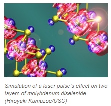
In experiments with the lab’s ultrafast ‘electron camera,’ laser light hitting a material is almost completely converted into nuclear vibrations, which are key to switching a material’s properties on and off for future electronics and other applications.
Materials that are only a few atomic layers thick have generated a lot of excitement in recent years. These 2-D materials can have intriguing properties, such as extraordinary mechanical strength and superior electrical and heat conductivity, and could benefit a number of next-generation applications, including flexible electronics, data storage devices, solar cells, light-emitting diodes and chemical catalysts. Researchers also think they may be able to customize the properties of these materials by using light pulses to rapidly switch them from one state, or phase, to another, for example from an insulating to a conducting state.
However, the ability to do this depends on how efficiently the light’s energy is transferred to the material’s atomic nuclei. Now, a team led by researchers from the Department of Energy’s SLAC National Accelerator Laboratory has demonstrated for the first time that the energy transfer is very fast and extremely efficient.
“Our data show that essentially all of the light energy gets converted into vibrations of the material's atomic nuclei within a trillionth of a second,” says SLAC’s Ming-Fu Lin, the lead author of a study published Nov. 23 in Nature Communications. “This efficient energy conversion is crucial, because those nuclear motions can initiate what we call a phase transition in the material – a change that alters its properties.”
The researchers looked at a sample made of two layers of molybdenum diselenide – a model system for 2-D materials that can potentially be switched from a semiconducting state to a metal state and vice versa. They first hit the sample with a very brief laser pulse and then observed how its energy spread into the material over time with SLAC’s ultrafast “electron camera” – an apparatus for ultrafast electron diffraction (UED) that uses a highly energetic electron beam to probe a sample’s atomic structure and nuclear motions.
"UED is a powerful tool for studies of these very thin 2-D materials," says SLAC staff scientist Xiaozhe Shen, a co-author of the paper. "The technique yields relatively strong signals, high spatial resolution, and it nicely complements X-ray laser studies in making movies of a material’s atomic structure.”
Although the researchers didn’t see a phase transition in molybdenum diselenide, their results help them better understand the energy transfer from the laser light to the material.
“It’s an important first step toward designing 2-D materials that we can control with light,” Lin says. “The next steps will be to find out if we can see light-induced phase transitions in other materials and if we can make materials whose properties we can alter in a controlled way by steering phase transitions in particular directions.”
The results are also used for the validation of novel software developed by the Materials Genome Innovation for Computational Software (MAGICS) center, led by the University of Southern California, Los Angeles. Another MAGICS partner involved in the study was Rice University, where the 2-D material was synthesized.
“Similar to biological genome projects that want to find out everything about the genomes of organisms, our goal is to learn everything about materials and to develop computational tools that allow us to make accurate predictions of material properties,” says SLAC’s Uwe Bergmann, the center’s associate director for validation and the principal investigator of the study. “MAGICS brings together researchers who develop advanced computer code, who take on the challenging synthesis of 2-D materials, and who provide the experimental data needed for testing the computer models. At SLAC, we’re doing UED experiments and ultrafast X-ray studies, but without the center’s team effort, this work wouldn’t be possible.”
Experiments for this study were carried out by researchers from SLAC’s Linac Coherent Light Source (LCLS), a DOE Office of Science User Facility; the Stanford PULSE Institute, which is jointly operated by SLAC and Stanford University; and the lab’s Accelerator Directorate. Samples came from Rice University, and computer simulations were done at USC. Additional MAGICS partners not involved in this study are DOE’s Lawrence Berkeley National Laboratory, the University of Missouri and the California Institute of Technology. The study was funded by the DOE Office of Science and the National Science Foundation.
Share on:


Suggested Items
Groundbreaking Ceremony Marks the Beginning of a New Era for Newccess Industrial; The Construction of the MINGXIN Building
04/12/2024 | Newccess IndustrialOn a clear and sunny day in March, the groundbreaking ceremony for the MINGXIN Building took place in Shenzhen, China. This moment marked the official commencement of construction for a project that will reshape the semiconductor materials industry.
The Need for a Holistic Global Sustainability Standard
04/10/2024 | Michael Ford, Aegis SoftwareNo one can deny that the resources of our fragile planet are finite. The environment seems like a third party, subject to constant degradation. We’re acutely aware of the effects of pollution on our climate, and despite our “throw-away” culture, recycling and recovery of materials has remained relatively expensive, even as we use more energy just to survive.
iNEMI Publishes Four Roadmap Topics
04/04/2024 | iNEMIThe International Electronics Manufacturing Initiative (iNEMI) announces the availability of the first roadmap topics in the new iNEMI Roadmap format. Printed circuit boards, sustainable electronics, smart manufacturing, and mmWave materials and test are now available online.
Insulectro’s 'Storekeepers' Extend Their Welcome to Technology Village at IPC APEX EXPO
04/03/2024 | InsulectroInsulectro, the largest distributor of materials for use in the manufacture of PCBs and printed electronics, welcomes attendees to its TECHNOLOGY VILLAGE during this year’s IPC APEX EXPO at the Anaheim Convention Center, April 9-11, 2024.
Checking In With ICAPE Group
04/03/2024 | Nolan Johnson, I-Connect007ICAPE Group’s field application engineer Erik Pederson drills down on sustainability, supply chain resiliency, and what value engineering really looks like in this exclusive interview. Founded in 1999, European-based ICAPE Group provides 21 million printed circuit boards and over six million technical parts to manufacturers every month. With 30 PCB manufacturing partners globally and 50 partners providing a wide array of technical parts, ICAPE Group has operations in China, Taiwan, Thailand, South Korea, Vietnam, South Africa, Europe, Mexico, and the United States. The company also focuses on the value proposition for its customers.