


 It’s Only Common Sense: OCCAM—the Time Is Now
 Marcy's Musings: The Growing Industry
 Dan’s Biz Bookshelf: Seeing the How
Fast Flowing Heat in Graphene Heterostructures
November 30, 2017 | ICFOEstimated reading time: 1 minute
Nanoscale heat flow plays a crucial role in many modern electronic and optoelectronic applications, such as thermal management, photodetection, thermoelectrics and data communication. Two-dimensional layered materials are beginning to confirm their groundbreaking role in many of these applications. Perhaps even more promising are so-called van der Waals heterostructures, consisting of different layered two-dimensional materials stacked one on top of the other. These stacks can consist of materials with dramatically different physical properties, while the interfaces between them are ultraclean and atomically sharp.
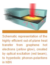
Scientists from the European Graphene Flagship, led by ICFO researchers, have recently succeeded in observing and following, in real-time, the way in which heat transport occurs in van der Waals stacks, which consist of graphene encapsulated by the dielectric two-dimensional material hexagonal BN (hBN).
In a study, recently published in Nature Nanotechnology entitled “Out-of-plane heat transfer in van der Waals stacks through electron–hyperbolic phonon coupling” , ICFO researchers Klaas-Jan Tielrooij, Niels C. H. Hesp, Mark B. Lundeberg, Mathieu Massicotte, Peter Schmidt, and Diana Davydovskaya, led by ICREA Prof at ICFO Frank Koppens, in collaboration with researchers from The Netherlands, Italy, Germany, and United Kingdom, have identified a highly surprisingly effect: rather than staying within the graphene sheet, the heat actually flows to the surrounding hBN sheets. This out-of-plane heat transfer process occurs on an ultrafast timescale of picoseconds (one millionth of a millionth of a second), and is therefore dominant over competing (in-plane) heat transfer processes.
The heat transfer process occurs through hot graphene electrons (experimentally generated by incident light) that couple to hyperbolic phonon-polaritons in the hBN sheets. These phonon-polaritons propagate within the hBN as light does in an optical fiber, but in this case for infrared wavelengths and at the nanometer scale. It turns out that these exotic hyperbolic modes are very efficient at carrying heat away.
The results of this work will definitely have far-reaching implications for many applications based on hBN-encapsulated graphene, sometimes referred to as the next generation graphene platform, owing to its superior electrical properties. In particular, it will provide direction to optoelectronic device design, where these heat flow processes can be thoroughly exploited.
Share on:


Suggested Items
SMC Korea 2024 to Highlight Semiconductor Materials Trends and Innovations on Industry’s Path to $1 Trillion
04/24/2024 | SEMIWith Korea a major consumer of semiconductor materials and advanced materials a key driver of innovation on the industry’s path to $1 trillion, industry leaders and experts will gather at SMC (Strategic Materials Conference) Korea 2024 on May 29 at the Suwon Convention Center in Gyeonggi-do, South Korea to provide insights into the latest materials developments and trends. Registration is open.
Groundbreaking Ceremony Marks the Beginning of a New Era for Newccess Industrial; The Construction of the MINGXIN Building
04/12/2024 | Newccess IndustrialOn a clear and sunny day in March, the groundbreaking ceremony for the MINGXIN Building took place in Shenzhen, China. This moment marked the official commencement of construction for a project that will reshape the semiconductor materials industry.
The Need for a Holistic Global Sustainability Standard
04/10/2024 | Michael Ford, Aegis SoftwareNo one can deny that the resources of our fragile planet are finite. The environment seems like a third party, subject to constant degradation. We’re acutely aware of the effects of pollution on our climate, and despite our “throw-away” culture, recycling and recovery of materials has remained relatively expensive, even as we use more energy just to survive.
iNEMI Publishes Four Roadmap Topics
04/04/2024 | iNEMIThe International Electronics Manufacturing Initiative (iNEMI) announces the availability of the first roadmap topics in the new iNEMI Roadmap format. Printed circuit boards, sustainable electronics, smart manufacturing, and mmWave materials and test are now available online.
Insulectro’s 'Storekeepers' Extend Their Welcome to Technology Village at IPC APEX EXPO
04/03/2024 | InsulectroInsulectro, the largest distributor of materials for use in the manufacture of PCBs and printed electronics, welcomes attendees to its TECHNOLOGY VILLAGE during this year’s IPC APEX EXPO at the Anaheim Convention Center, April 9-11, 2024.