


 Happy’s Tech Talk #28: The Power Mesh Architecture for PCBs
 It’s Only Common Sense: Would You Join Your Own Company?
 The Chemical Connection: Reducing Etch System Water Usage, Part 2
New Nanowires are Just a Few Atoms Thick
December 5, 2017 | MITEstimated reading time: 3 minutes
“Two-dimensional materials” — materials deposited in layers that are only a few atoms thick — are promising for both high-performance electronics and flexible, transparent electronics that could be layered onto physical surfaces to make computing ubiquitous.
The best-known 2-D material is graphene, which is a form of carbon, but recently researchers have been investigating other 2-D materials, such as molybdenum disulfide, which have their own, distinct advantages.
Producing useful electronics, however, requires integrating multiple 2-D materials in the same plane, which is a tough challenge. In 2015, researchers at King Abdullah University in Saudi Arabia developed a technique for depositing molybdenum disulfide (MoS2) next to tungsten diselenide (WSe2), with a very clean junction between the two materials. With a variation of the technique, researchers at Cornell University then found that they could induce long, straight wires of MoS2 — only a few atoms in diameter— to extend into the WSe2, while preserving the clean junction.
The researchers contacted Markus Buehler, the McAfee Professor of Engineering in MIT’s Department of Civil and Environmental Engineering, who specializes in atomic-level models of crack propagation, to see if his group could help explain this strange phenomenon.
In the latest issue of Nature Materials, the King Abdullah, Cornell, and MIT researchers team with colleagues at Academia Sinica, the Taiwanese national research academy, and Texas Tech University to describe both the material deposition method and the mechanism underlying the formation of the MoS2 nanowires, which the MIT researchers were able to model computationally.
“The manufacturing of new 2-D materials still remains a challenge,” Buehler says. “The discovery of mechanisms by which certain desired material structures can be created is key to moving these materials toward applications. In this process, the joint work of simulation and experiment is critical to make progress, especially using molecular-level models of materials that enable new design directions.”
Wired up
The ability to create long, thin MoS2 channels in WSe2 could have a number of applications, the researchers say.
“Based on [the materials’] electrical properties and optical properties, people are looking at using MoS2 and WSe2 for solar cells or for water splitting based on sunlight,” says Gang Seob Jung, an MIT graduate student in civil and environmental engineering and a coauthor on the new paper. “Most of the interesting stuff happens at the interface. When you have not just the one interface — if there are many nanowire interfaces — it could improve the efficiency of a solar cell, even if it’s quite random.”
But the theoretical explanation of the molecular mechanism underlying the nanowires’ formation also raises the hope that their formation could be controlled, to enable the assembly of atom-scale electronic components.
“Two-D materials, one of the most promising candidates for future electronics, ultimately need to beat silicon-based devices, which have achieved a few nanometers in size already,” says Yimo Han, a Cornell graduate student in chemistry and first author on the paper. “Two-D materials are the thinnest in the vertical direction but still span a quite large area in the lateral dimensions. We made the thinnest dislocation-free channels in 2-D materials, which is a big step toward subnanometer electronic devices out of 2-D materials.”
Propagating polygons
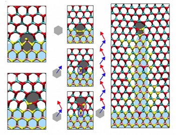
In a 2-D crystal, both MoS2 and WSe2 naturally arrange themselves into hexagons in which the constituent elements — molybdenum and sulfur or tungsten and selenium — alternate. Together, these hexagons produce a honeycomb pattern.
The Cornell researchers’ fabrication technique preserves this honeycomb pattern across the junction between materials, a rare feat and one that’s very useful for electronics applications. Their technique uses chemical vapor deposition, in which a substrate — in this case, sapphire — is exposed to gases carrying chemicals that react to produce the desired materials.
The natural sizes of the MoS2 and WSe2 hexagons are slightly different, however, so their integration puts a strain on both crystals, particularly near their junction. If a pair of WSe2 hexagons right at the MoS2 junction convert into a hexagon matched with a heptagon (a seven-sided polygon), it releases the strain.
This so-called 5|7 dislocation creates a site at which an MoS2 particle can attach itself. The resulting reaction inserts a molybdenum atom into the pentagon, producing a hexagon, and breaks the heptagon open. Sulfur atoms then attach to the heptagon to form another 5|7 dislocation. As this process repeats, the 5|7 dislocation moves deeper into WSe2 territory, with a nanowire extending behind it. The pattern in which the strain on the mismatched hexagons relaxes and recurs ensures that the dislocation progresses along a straight line.
The research was supported by the Office of Naval Research and the Department of Defense.
Share on:


Suggested Items
AIM Solder Signs Shinil Fl Ltd. as New Distributor for Korea
05/08/2024 | AIM SolderAIM Solder, a leading global manufacturer of solder assembly materials for the electronics industry, is pleased to announce a new distribution partnership with Shinil Fl Ltd., a prominent supplier of technological solutions in the SMT and semiconductor sectors.
KYZEN’s Adam Klett to Keynote at SMTA Electronics in Harsh Environments Conference
05/07/2024 | KYZEN'KYZEN, the global leader in innovative environmentally friendly cleaning chemistries, announced today that KYZEN’s Director of Science, Adam Klett, PhD will present as a keynote speaker at the SMTA Electronics in Harsh Environments Conference. The event is scheduled to take place May 14-16, 2024 at the Technical University of Denmark in Copenhagen, Denmark.
Altus Equips SSTL with Advanced Cleaning Technology for Electronics
05/07/2024 | Altus GroupAltus Group, a leading supplier of capital equipment for the electronics manufacturing industry, has announced the successful installation of an advanced PCBA cleaning system at Surrey Satellite Technology Limited (SSTL).
GPV's Handover of Refurbished Factory Building
05/07/2024 | GPVOn 6 May 2024, Bjorn Fiskers, MD at GPV Electronics TH in Thailand and his team were handed the keys to our refurbished factory building, adding another 7,000 sqm to our current 15,000 sqm electronics factory. Our electronics factory in Thailand will comprise of a total of 22,000 sqm.
New Yorker, Major League Electronics Sign New Franchised Distribution Agreement
05/06/2024 | New Yorker Electronics Co.New Yorker Electronics, global distributor of electronic components, recently announced a new franchised distribution agreement with Major League Electronics, renowned manufacturer of interconnect products.