


 The Right Approach: I Hear the Train A Comin'
 It’s Only Common Sense: OCCAM—the Time Is Now
 Marcy's Musings: The Growing Industry
UNIST Researchers Develop Silicon Chip-based Quantum Photonic Devices
December 12, 2017 | UNISTEstimated reading time: 3 minutes
An international team of researchers, affiliated with UNIST has presented a core technology for quantum photonic devices used in quantum information processing. They have proposed combining of quantum dots for generating light and silicon photonic technologies for manipulating light on a single device.
This breakthrough has been led by Professor Je-Hyung Kim in the School of Natural Science at UNIST in collaboration with Professor Edo Waks and a group of researchers at the University of Maryland, United States.
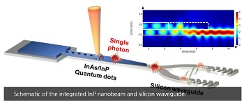
In this study, the research team demonstrated the integration of silicon photonic devices with a solid-state single photon emitter. We use a hybrid approach that combines silicon photonic waveguides with InAs/InP quantum dots that act as efficient sources of single photons at telecom wavelengths spanning the O-band and C-band.
Nano letters 2Schematic of the integrated InP nanobeam and silicon waveguide.
In classical computing, a bit is a single piece of information that can exist in two states – 1 or 0. Quantum computers uses quantum bits that can occupy 0, 1, or a a superposition that can be both at the same time. Although there are several potentially fruitful approaches exist to quantum information processing based on a variety of quantum technologies, including atom, light, and superconducting devices. However, the future of quantum computing, like the quantum state itself, still remains uncertain. Professor Kim focuses on the quantum information processing, using light. This is because quantum bits can be implemented using the polarized state of light, its duration, and the route information, similar to electron spins.
A recently developed quantum light source exhibits the characteristics of quantum physics, including the superposition, quantum entanglement, and no-cloning theorem. This has enabled innovative application technologies, such as quantum simulators, quantum state transfer, and quantum cryptography. However, in order to commercialize the technologies used for the actual quantum information processing technology, it is necessary to perform quantum optics experiments directly on the photonic device. According to the research team, such innovation could be the precursor for quantum circuits, which are expected to play a large role in the future of quantum computers and communication.
“In order to build photon-based integrated quantum optical devices, it is necessary to produce as many quantum light sources as possible in a single chip,” says Professor Kim. “Through this study, we have proposed the basic form of quantum optical devices by producing highly effective quantum light source with quantum dots and creating the pathway to manipulate light with the use of silicon substrates.”
A scanning electron microscope image of the fabricated nanobeam that is suspended by thin tethers that attach it to the bulk substrate.A scanning electron microscope image of the fabricated nanobeam that is suspended by thin tethers that attach it to the bulk substrate.
Quantum dots are ultrafine particles or nanocrystals of a semiconductor material with fiameters in the range of 2 to 10 nanometers (A nanometer is one billionth of a meter). In general, quantum dots take the form of compounds. However, as the size decreases, they begin to exhibit discontinuous energy structure, which results in having similar properties to the light emitted by atoms. Although quantum dots have been used successfully as highly efficient single-photon sources, they had difficulty controlling light.
In the study, the research team demonstrated the integration of silicon photonic devices with a solid-state single photon emitter. Here, they used a hybrid approach that combines silicon photonic waveguides with InAs/InP quantum dots that act as efficient sources of single photons at telecom wavelengths spanning the O-band and C-band. Then, they removed the quantum dots via a pick-and-place procedure with a microprobe tip combined with a focused ion beam and scanning electron microscope. This technique allowed transferring of tapered InP nanobeams containing InAs quantum dots onto a silicon waveguide with nanometer-scale precision.
“This integration opens up the possibility to leverage the highly advanced photonics capabilities developed in silicon to control and route nonclassical light from on-demand single photon sources,” the research team notes. “In addition, the fabricated devices operate at telecom wavelengths and can be electrically driven, which are useful for fiber-based quantum communication.”
The quantum optical device, developed by the research team has successfully transferred the emission from the quantum dots along the silicon photonic circuits with high efficiency. Using this, they also successfully incorporate an on-chip silicon-photonic beamsplitter to perform a Hanbury-Brown and Twiss measurement.
“Our approach could enable integration of precharacterized III–V quantum photonic devices into large-scale photonic structures to enable complex devices composed of many emitters and photons,” says Professor Kim.
Share on:


Suggested Items
Stan Rak: Elevating the Ideas and Insights of IPC's Thought Leaders Program
04/25/2024 | Stanton Rak, SF Rak CompanyAs a member of the IPC Thought Leaders Program (TLP), I am responsible for identifying knowledge-sharing opportunities that can generate ideas and insights that strengthen the IPC community as well as create a sustainable and lasting future for its members. I am delighted to highlight some of my recent contributions as a member of the TLP.
indie Semiconductor Launches Advanced Smart Connectivity Solutions for In-Cabin Applications
04/23/2024 | indie Semiconductorindie Semiconductor, Inc., an Autotech solutions innovator, has introduced a family of new high-performance video converters and retimers to enable in-cabin connectivity applications, including audio and video transport and device interfacing.
The Need for a Holistic Global Sustainability Standard
04/10/2024 | Michael Ford, Aegis SoftwareNo one can deny that the resources of our fragile planet are finite. The environment seems like a third party, subject to constant degradation. We’re acutely aware of the effects of pollution on our climate, and despite our “throw-away” culture, recycling and recovery of materials has remained relatively expensive, even as we use more energy just to survive.
Technica Leads the Way Into Automation and Machine Learning at IPC APEX EXPO 2024
03/28/2024 | Marcy LaRont, PCB007 MagazineAs a significant partner to PCB fabricators since almost the beginning of multilayer boards, Technica USA brings a lot of expertise to the industry. This year’s IPC APEX EXPO show will showcase their biggest booth yet, and a whole lot of information, discussion and demonstration around automation and AI machine learning. In this interview, Jason Perry discusses Technica's plans for the show, and why attendees should stop by.
Airbus to Acquire INFODAS and Strengthen its Cybersecurity Portfolio
03/25/2024 | AirbusAirbus Defence and Space has entered into an agreement to acquire INFODAS, a Cologne-based, German company that provides cybersecurity and IT solutions in the public sector including for defence and critical infrastructures.