


 Happy’s Tech Talk #28: The Power Mesh Architecture for PCBs
 It’s Only Common Sense: Would You Join Your Own Company?
 The Chemical Connection: Reducing Etch System Water Usage, Part 2
Artificial Graphene in a Nanofabricated Semiconductor Structure
December 18, 2017 | Columbia UniversityEstimated reading time: 4 minutes
Researchers at Columbia Engineering, experts at manipulating matter at the nanoscale, have made an important breakthrough in physics and materials science, recently reported in Nature Nanotechnology. Working with colleagues from Princeton and Purdue Universities and Istituto Italiano di Tecnologia,the team has engineered “artificial graphene” by recreating, for the first time, the electronic structure of graphene in a semiconductor device.
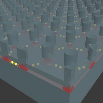
Image caption: Nanofabrication of artificial graphene in a semiconductor. The green layer represents the 2D sheet where the electrons can move. Nanolithography and etching form small pillars beneath which lie the quantum dots arranged in an hexagonal lattice. Scanning electron micrographs at the bottom show the hexagonal array, with a period of only 50 nanometers, from the top and at an angle. —Diagram credit: Lingjie Du/Columbia Engineering
“This milestone defines a new state-of-the-art in condensed matter science and nanofabrication,” says Aron Pinczuk, professor of applied physics and physics at Columbia Engineering and senior author of the study. “While artificial graphene has been demonstrated in other systems such as optical, molecular, and photonic lattices, these platforms lack the versatility and potential offered by semiconductor processing technologies. Semiconductor artificial graphene devices could be platforms to explore new types of electronic switches, transistors with superior properties, and even, perhaps, new ways of storing information based on exotic quantum mechanical states.”
The discovery of graphene in the early 2000s generated tremendous excitement in the physics community not only because it was the first real-world realization of a true two-dimensional material but also because the unique atomic arrangement of the carbon atoms in graphene provided a platform for testing new quantum phenomena that are difficult to observe in conventional materials systems. With its unusual electronic properties—its electrons can travel great distances before they are scattered—graphene is an outstanding conductor. These properties also display other unique characteristics that make electrons behave as if they are relativistic particles that move close to the speed of light, conferring upon them exotic properties that “regular,” non-relativistic electrons do not have.
But graphene, a natural substance, comes in only one atomic arrangement: the positions of the atoms in the graphene lattice are fixed,and thu sall experiments on graphene must adapt to those constraints. On the other hand, in artificial graphene the lattice can be engineered over a wide range of spacings and configurations, making it a holy grail of sorts for condensed matter researchers because it will have more versatile properties than the natural material.
“This is a rapidly expanding area of research, and we are uncovering new phenomena that couldn’t be accessed before,” says Shalom Wind, faculty member of the department of applied physics and applied mathematics and co-author of the study. “As we explore novel device concepts based on electrical control of artificial graphene, we can unlock the potential to expand frontiers in advanced optoelectronics and data processing.”
“This work is really a major advance in artificial graphene. Since the first theoretical prediction that system with graphene-like electronic properties may be artificially created and tuned with patterned 2D electron gas, no one had succeeded, until the Columbia work, in directly observing these characteristics in engineered semiconductor nanostructures,” says Steven G. Louie, professor of physics, University of California, Berkeley, who was not involved in the study. “Previous work with molecules, atoms, and photonic structures represent far less versatile and stable systems. The nanofabricated semiconductor structures open up tremendous opportunities for exploring exciting new science and practical applications.”
The researchers used the tools of conventional chip technology to develop the artificial graphene in a standard semiconductor material, gallium arsenide. They designed a layered structure so that the electrons could move only within a very narrow layer, effectively creating a 2D sheet. They used nanolithography and etching to pattern the gallium arsenide: the patterning created a hexagonal lattice of sites in which the electrons were confined in the lateral direction. By placing these sites, which could be thought of as “artificial atoms,” sufficiently close to one another (~ 50 nanometers apart), these artificial atoms could interact quantum mechanically, similar to the way atoms share their electrons in solids.
The team probed the electronic states of the artificial lattices by shining laser light on them and measuring the light that was scattered. The scattered light showed a loss of energy that corresponded to transitions in the electron energy from one state to another. When they mapped these transitions, the team found that they were approaching zero in a linear fashion around what is called the “Dirac point” where the electron density vanishes, a hallmark of graphene.
This artificial graphene has several advantages over natural graphene: for instance, researchers can design variations into the honeycomb lattice to modulate electronic behavior. And because the spacing between the quantum dots is much larger than the inter-atomic spacing in natural graphene, researchers can observe even more exotic quantum phenomena with the application of a magnetic field.
The discovery of new low-dimensional materials, such as graphene and other ultrathin, layered van der Waals films that exhibit exciting new physical phenomena that were previously inaccessible, laid the groundwork for this study. “What was really critical to our work was the impressive advancements in nanofabrication,” Pinczuk notes. “These offer us an ever-increasing toolbox for creating a myriad of high-quality patterns at nanoscale dimensions. This is an exciting time to be a physicist working in our field.”
—by Holly Evarts
Share on:


Suggested Items
KYZEN’s Adam Klett to Keynote at SMTA Electronics in Harsh Environments Conference
05/07/2024 | KYZEN'KYZEN, the global leader in innovative environmentally friendly cleaning chemistries, announced today that KYZEN’s Director of Science, Adam Klett, PhD will present as a keynote speaker at the SMTA Electronics in Harsh Environments Conference. The event is scheduled to take place May 14-16, 2024 at the Technical University of Denmark in Copenhagen, Denmark.
Altus Equips SSTL with Advanced Cleaning Technology for Electronics
05/07/2024 | Altus GroupAltus Group, a leading supplier of capital equipment for the electronics manufacturing industry, has announced the successful installation of an advanced PCBA cleaning system at Surrey Satellite Technology Limited (SSTL).
GPV's Handover of Refurbished Factory Building
05/07/2024 | GPVOn 6 May 2024, Bjorn Fiskers, MD at GPV Electronics TH in Thailand and his team were handed the keys to our refurbished factory building, adding another 7,000 sqm to our current 15,000 sqm electronics factory. Our electronics factory in Thailand will comprise of a total of 22,000 sqm.
Worldwide Silicon Wafer Shipments Dip 5% in Q1 2024
05/07/2024 | SEMIWorldwide silicon wafer shipments decreased 5.4% quarter-over-quarter to 2,834 million square inches in the first quarter of 2024, a 13.2% drop from the 3,265 million square inches recorded during the same quarter last year, the SEMI Silicon Manufacturers Group (SMG) reported in its quarterly analysis of the silicon wafer industry.
New Yorker, Major League Electronics Sign New Franchised Distribution Agreement
05/06/2024 | New Yorker Electronics Co.New Yorker Electronics, global distributor of electronic components, recently announced a new franchised distribution agreement with Major League Electronics, renowned manufacturer of interconnect products.