


 It’s Only Common Sense: OCCAM—the Time Is Now
 Marcy's Musings: The Growing Industry
 Dan’s Biz Bookshelf: Seeing the How
Electron Injection Transforms a Thin Film
December 20, 2017 | Department of Energy, Office of ScienceEstimated reading time: 2 minutes
If you want to change how a material handles electrons, re-arrange the atoms. Scientists found a reversible way to alter the atom’s arrangement. Recently, researchers predicted that injecting electrons into a thin film could build up enough energy to move atoms (altering the crystal structure) and change the material’s properties.
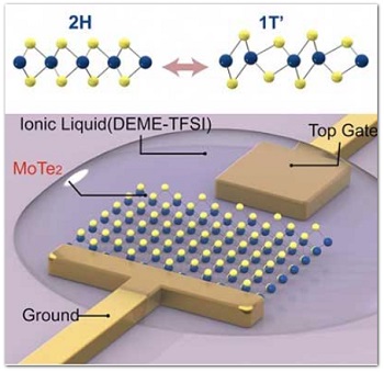
Image caption: Bringing us closer to advanced computer memory, new research using “electron injections” reversibly changes the crystal structure of a 2-D semiconductor. In all materials, the crystal structure determines the electronic properties. The artist’s rendering shows a single atomic layer of molybdenum ditelluride (blue/yellow spheres; MoTe2). This 2-D semiconductor is sandwiched between electrodes and covered by an ionic liquid droplet that stores electrical charge. When a small voltage is applied, electrons are “injected” and the structure is transformed from a “2H” to a more slanted “1T’” arrangement (top). (Image: Lawrence Berkeley National Laboratory)
Now, a team proved this prediction correct. Simple electron injections reversibly change the crystal structure of atomically thin films of a common semiconductor. This method to change the crystal structure uses far less energy than heating or chemical processes (Nature, "Structural phase transition in monolayer MoTe2 driven by electrostatic doping").
To create atomically thin computer memory, scientists are studying certain ultra-thin semiconductors. These thin films are based on a class of materials called transition-metal dichalcogenides. The films have unique properties. The team’s discovery about electron injections opens up options for creating designer films. The films are of interest for advanced computers and solar panels.
Monolayer thin films of 2-D, transition-metal dichalcogenides have emerged as important materials with unique properties, drawing great attention in science and technology. Of particular interest are their electronic and optical properties. The electrical properties can vary between no electrical resistance to unique spin-related electrical transport properties.
Validating theoretical predictions, researchers reported an experimental demonstration which suggested that the simple application of a small voltage could be used to induce a structural phase transformation in an atomically thin film of molybdenum ditelluride (MoTe2).
The semiconductor film was coated with an ionic liquid that stores electric charges and controls the charge injection to the atomically thin film. Electrons accumulated in the film through a process called electrostatic doping, similar to traditional chemical doping, where the addition of a small amount of dopant changes the electronic properties of a material. But here, electrons’ injection is dynamic and clean, without creating defects.
In response to the electrostatic doping, the atoms rearranged themselves in the film. The rearrangement formed a different crystal structure, which was metallic. The electrostatic doping made the crystal structure more slanted.
While varying the gate voltage, the researchers used spectroscopic techniques (Raman scattering and second-harmonic generation) to monitor changes in the film. When the dopant electrons were removed from the film, by lowering the voltage, the original crystal structure returned. The structural transformations were reversible and uniform across the whole sample.
This simple method controls the crystal structure and alters the electronic properties between 2-D semiconductors and semi-metals. It opens up exciting possibilities in the development of new, phase-change devices.
Share on:


Suggested Items
Knightscope Caps Off Year with 6-Robot Expansion Contract
01/02/2024 | BUSINESS WIREKnightscope, Inc., a leading developer of autonomous security robots and blue light emergency communication systems, today announces a new expansion contract for 6 Autonomous Security Robots (ASRs) including 2 of its 5th Generation K5s and 4 K1 Hemispheres, bringing the total number of robots under contract for this client to 14.
Elementary, Mr. Watson: Slash Sheets a ‘Smorgasbord’ of Materials
05/15/2023 | John Watson -- Column: Elementary, Mr. WatsonSlash sheets touch on materials, one of my favorite areas of PCB design, and what I refer to as “the buffet of the PCB world.” After all, this smorgasbord of materials comes in an endless variety, with differing balances of reinforcement and resin, from different manufacturers and vendors, and from a variety of sources. Add the possibility of out-of-date or deteriorated panels, and it makes ensuring the quality of your next PCB design a real hit or miss.
Pusan National University Researchers Develop Way to Tune Energy Levels of Semimetals
03/28/2023 | PRNewswireType-II Dirac semimetals are quantum materials with unique energy level structures, such as a bulk Dirac point (BDP). However, these semimetals are unsuitable for real-life applications because their BDP is far off the "Fermi energy level."
WPI-MANA Demystifies Conductivity of Ruthenate Nanosheets, Moving Towards Next-generation Electronics
02/17/2023 | PRNewswireA research team at the International Center for Materials Nanoarchitectonics (WPI-MANA) has shed light on how electrical conduction in oxide nanosheets can be markedly affected by small changes in their atomic arrangement.
New Data Extracted from Old for Materials Databases
11/07/2022 | ACN NewswireA new approach uses data from one type of test on small metal alloy samples to extract enough information for building databases that can be used to predict the properties and potentials of new materials.