


 The Right Approach: I Hear the Train A Comin'
 It’s Only Common Sense: OCCAM—the Time Is Now
 Marcy's Musings: The Growing Industry
Atomically Thin Perovskites Boost for Future Electronics
December 29, 2017 | National Institute for Materials ScienceEstimated reading time: 1 minute
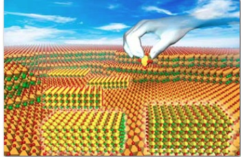
WPI-MANA has developed the world's highest performance dielectric nanofilms using atomically thin perovskites (JACS, "Atomic Layer Engineering of High-κ Ferroelectricity in 2D Perovskites"). This technology may revolutionize the next-generation of electronics.
Image caption: Complex perovskite oxides offer tremendous potential for controlling their rich variety of electronic properties, including high-TC superconductivity, high-κ ferroelectricity, and quantum magnetism. Atomic-scale control of these intriguing properties in ultrathin perovskites is an important challenge for exploring new physics and device functionality at atomic dimensions. (ACS)
This research was conducted by a WPI-MANA research group led by Principal Investigator Minoru Osada and Director Takayoshi Sasaki of WPI-MANA at NIMS. Electronic devices are getting smaller all the time, but there is a limit to how small they can get using current materials and technology. High-κ dielectric materials may be the key for developing electronic devices of the future.
Minoru Osada and colleagues created high-performance dielectric nanofilms using 2D perovskite nanosheets (Ca2Nam-3NbmO3m+1; m = 3–6) as building blocks. Perovskite oxides offer tremendous potential for controlling their rich variety of electronic properties including high-κ dielectric and ferroelectric.
The researchers demonstrated the targeted synthesis of nanofilms composed of 2D perovskite nanosheets in a unit-cell-upon-unit-cell manner. In this unique system, perovskite nanosheets enable precise control over the thickness of the perovskite layers in increments of ∼0.4 nm (one perovskite unit) by changing m, and such atomic layer engineering enhances the high-κ dielectric response and local ferroelectric instability. The m = 6 member (Ca2Na3Nb6O19) attained the highest dielectric constant, εr = ∼470, ever realized in all known dielectrics in the ultrathin region of less than 10 nm.
Perovskite nanosheets are of technological importance for exploring high-κ dielectrics in 2D materials, which have great potential in electronic applications such as memories, capacitors, and gate devices.
Notably, perovskite nanosheets afforded high capacitances by relying on high-κ values at a molecular thickness. Ca2Na3Nb6O19 exhibited an unprecedented capacitance density of approximately 203 µF cm-2, which is about three orders of magnitude greater than that of currently available ceramic condensers, opening a route to ultra-scaled high-density capacitors.
These results provide a strategy for achieving 2D high-κ dielectrics/ferroelectrics for use in ultra-scaled electronics and post-graphene technology.
Share on:


Suggested Items
Warm Windows and Streamlined Skin Patches – IDTechEx Explores Flexible and Printed Electronics
04/26/2024 | IDTechExFlexible and printed electronics can be integrated into cars and homes to create modern aesthetics that are beneficial and easy to use. From luminous car controls to food labels that communicate the quality of food, the uses of this technology are endless and can upgrade many areas of everyday life.
Book Excerpt: The Printed Circuit Assembler’s Guide to... Factory Analytics
04/24/2024 | I-Connect007 Editorial TeamIn our fast-changing, deeply competitive, and margin-tight industry, factory analytics can be the key to unlocking untapped improvements to guarantee a thriving business. On top of that, electronics manufacturers are facing a tremendous burden to do more with less. If you don't already have a copy of this book, what follows is an excerpt from the introduction chapter of 'The Printed Circuit Assembler’s Guide to... Factory Analytics: Unlocking Efficiency Through Data Insights' to whet your appetite.
Listen Up! The Intricacies of PCB Drilling Detailed in New Podcast Episode
04/25/2024 | I-Connect007In episode 5 of the podcast series, On the Line With: Designing for Reality, Nolan Johnson and Matt Stevenson continue down the manufacturing process, this time focusing on the post-lamination drilling process for PCBs. Matt and Nolan delve into the intricacies of the PCB drilling process, highlighting the importance of hole quality, drill parameters, and design optimization to ensure smooth manufacturing. The conversation covers topics such as drill bit sizes, aspect ratios, vias, challenges in drilling, and ways to enhance efficiency in the drilling department.
Elevating PCB Design Engineering With IPC Programs
04/24/2024 | Cory Blaylock, IPCIn a monumental stride for the electronics manufacturing industry, IPC has successfully championed the recognition of the PCB Design Engineer as an official occupation by the U.S. Department of Labor (DOL). This pivotal achievement not only underscores the critical role of PCB design engineers within the technology landscape, but also marks the beginning of a transformative journey toward nurturing a robust, skilled workforce ready to propel our industry into the future.
Winner of The Science Show Rakett 69 Receives Incap Scholarship
04/24/2024 | IncapThe winner of the Rakett 69 science show, Andri Türkson, who stood out as an electronics enthusiast, received a scholarship from Incap Estonia, along with an internship opportunity in Saaremaa.