


 Marcy's Musings: The Growing Industry
 It’s Only Common Sense: Here’s What To Do After IPC APEX EXPO 2024
 Dan’s Biz Bookshelf: Seeing the How
Viewing Atomic Structures of Dopant Atoms in 3-D Relating to Electrical Activity in a Semiconductor
December 29, 2017 | Tokyo Institute of TechnologyEstimated reading time: 3 minutes
Scientists at Tokyo Institute of Technology (Tokyo Tech) and their research team involving researchers of JASRI, Osaka University, Nagoya Institute of Technology, and Nara Institute of Science and Technology have just developed a novel approach to determine and visualize the three-dimensional (3D) structure of individual dopant atoms using SPring-8. The technique will help improve the current understanding of the atomic structures of dopants in semiconductors correlated with their electrical activity and thus help support the development of new manufacturing processes for high-performance devices.
Using a combination of spectro-photoelectron holography, electrical property measurements, and first-principles dynamics simulations, the 3D atomic structures of dopant impurities in a semiconductor crystal were successfully revealed. The need for a better understanding of the atomic structures of dopants in semiconductors had been long felt, mainly because the current limitations on active dopant concentrations result from the deactivation of excess dopant atoms by the formation of various types of clusters and other defect structures.
The search for techniques to electrically activate the dopant impurities in semiconductors with high efficiency and/or at high concentrations have always been an essential aspect of semiconductor device technology. However, despite various successful developments, the achievable maximum concentration of active dopants remains limited. Given the impact of the dopant atomic structures in this process, these structures had been previously investigated using both theoretical and experimental approaches. However, direct observation of the 3D structures of the dopant atomic arrangements had hitherto been difficult to achieve.
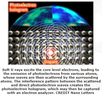
In this study, Kazuo Tsutsui at Tokyo Tech and colleagues involving researchers at JASRI, Osaka University, Nagoya Institute of Technology, and Nara Institute of Science and Technology developed spectro-photoelectron holography using SPring-8, and leveraged the capabilities of photoelectron holography in determining the concentrations of dopants at different sites, based on the peak intensities of the photoelectron spectrum, and classified electrically active / inactive atomic sites. These structures directly related with the density of carriers. In this approach, soft X-ray excitation of the core level electrons leads to the emission of photoelectrons from various atoms, whose waves are then scattered by the surrounding atoms. The resulting interference pattern creates the photoelectron hologram, which may then be captured with an electron analyzer. The photoelectron spectra acquired in this manner contain information from more than one atomic site. Therefore, peak fitting is performed to obtain the photoelectron hologram of individual atomic sites. The combination of this technique with first-principles simulations allows the successful estimation of the 3D structure of the dopant atoms, and the assessment of their different chemical bonding states. The method was used to estimate the 3D structures of arsenic atoms doped onto a silicon surface. The obtained results fully demonstrated the power of the proposed method and allowed confirmation of several previous results.
This work demonstrates the potential of spectro-photoelectron holography for the analysis of impurities in semiconductors. This technique allows analyses that are difficult to perform with conventional approaches and should therefore be useful in the development of improved doping techniques and, ultimately, in supporting the manufacture of high-performance devices.
About Tokyo Institute of Technology
Tokyo Institute of Technology stands at the forefront of research and higher education as the leading university for science and technology in Japan. Tokyo Tech researchers excel in a variety of fields, such as material science, biology, computer science and physics. Founded in 1881, Tokyo Tech has grown to host 10,000 undergraduate and graduate students who become principled leaders of their fields and some of the most sought-after scientists and engineers at top companies. Embodying the Japanese philosophy of "monotsukuri," meaning technical ingenuity and innovation, the Tokyo Tech community strives to make significant contributions to society through high-impact research.
Share on:


Suggested Items
IDTechEx Explores the Role of 3D Cu-Cu Hybrid Bonding in Powering Future HPC and AI Products
04/18/2024 | PRNewswireSemiconductor packaging has evolved from traditional 1D PCB levels to cutting-edge 3D hybrid bonding at the wafer level, achieving interconnecting pitches as small as single micrometers and over 1000 GB/s bandwidth. Key parameters, including Power, Performance, Area, and Cost, are crucial considerations
Intel Brings AI-Platform Innovation to Life at the Olympic Games
04/18/2024 | BUSINESS WIREIntel announced its plans for the Olympic and Paralympic Games Paris 2024. Bringing AI Everywhere, Intel will implement artificial intelligence technology powered by Intel processors on the world’s biggest stage.
Adura Solutions Exhibits at Del Mar 2024
04/18/2024 | Adura SolutionsSumit Tomar, CEO of Adura Solutions, has announced that his company will be exhibiting at this year's Del Mar Electronics and Manufacturing Show to be held at the Del Mar Fairgrounds, San Diego, California, April 24-25.
Australian Flow Batteries and The SCHMID Group Announce Groundbreaking Memorandum of Understanding
04/17/2024 | SCHMID GroupAustralian Flow Batteries Pty Ltd (AFB), a leader in innovative energy solutions and economical, safe, and reliable power storage, and SCHMID Energy Systems GmbH a company of the German SCHMID Group, a global technology leader with a rich history in delivering innovative solutions across multiple industries including Electronics, Renewables, and Energy Storage sectors, are thrilled to announce the signing of a Memorandum of Understanding (MoU)
Ansys Joins BAE Systems’ Mission Advantage Program to Advance Digital Engineering Across US Department of Defense
04/16/2024 | ANSYSAnsys announced it is working with BAE Systems, Inc., to accelerate the adoption of digital engineering and MBSE across the Department of Defense (DoD).