


 It’s Only Common Sense: OCCAM—the Time Is Now
 Marcy's Musings: The Growing Industry
 Dan’s Biz Bookshelf: Seeing the How
Bendable Touch Panel Achieved with Silver Nano Ink Printing Technology
January 17, 2018 | ACN NewswireEstimated reading time: 4 minutes
JST has recognized the results of NexTEP's project, "A Sensor Film for Touch Panels Using Thin Metallic Wire" as a success.
This development task was based on the research of Professor Tatsuo Hasegawa, Principal Research Manager at the Flexible Electronics Research Center of the National Institute of Advanced Industrial Science and Technology, and was consigned to Tanaka Kikinzoku Kogyo (Representative Director & CEO, Akira Tanae, Chiyoda-ku, Tokyo) from April 2014 through September 2017. The research proceeded with the aim of practical application through Tanaka Kikinzoku Kogyo's Global Marketing/R&D Division.
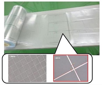
In conventional electrostatic capacity-type touch panels, indium tin oxide (ITO) is used for the sensor. However, because of its high electrical resistivity and weakness upon bending, companies faced difficulties in increasing the size of such sensors and making them more flexible. Metal mesh (MM) solves these problems, but it is difficult to make thinner than 4 um, and no technology existed to manufacture the mesh via printing.
To apply the new technology (SuPR-NaP method), which fabricates wiring through an adsorption reaction between special silver ink and an activated fluororesin surface, at a suitable speed for commercial manufacturing, the project clarified the reaction mechanism and researched the development of manufacturing equipment as well as the conditions for each process. As a result, the project constructed a system for manufacturing MM film (line width: 2-4 um) with the full process roll-to-roll method*5. In a 200,000-frequency (radius: 2 mm) bending test, this MM film exhibits hardly any changes in resistance values, and it has cleared general reliability testing.
This success in manufacturing the world's first micro-wiring film with a full process roll-to-roll method is an important technological innovation in printed electronics for the flexible electronic device market. It is also anticipated that the technology could be applied and used for applications requiring metal patterns on resin film (function films e.g. antibacterial, catalyst, thermal insulating).
With the increased use of information technology in society, people are demanding access to information in various locations, at various times and in various situations. Touch panels that are integrated with the display are used in many devices, from smartphones, notebooks, large panel to automotive displays.
Moreover, touch sensors now need to be compatible with not only flat panel displays, but also recently-announced three-dimensional curved and bendable displays. Transparent (conducting) electrodes using ITO are mainly used for current touch sensors. However, physical problems such as high electrical resistivity and weakness upon bending imposed limitations on responding to needs for flexibility and increasingly large screen sizes. Metal mesh(MM), in which thin metallic wire is used as the electrode, is being applied on as a material that could solve these problems. However, as the line width and pitch of current MM is thick, the wiring is visible on smartphones, which are used at a short distance. Therefore, it has only come into popular use for large displays.
Development Details
With this new printing technology, a film to which liquid-repelling fluororesin is applied undergoes pattern exposure through a photo mask. Metal ink is then scanned onto it to form the wiring. This technology means that metal wiring with a fixed film thickness can be formed by means of the chemisorption of metal nanoparticles on the fluororesin surface activated by light.
The following technology has been developed to make it possible to manufacture MM film with micro wiring that can also be used for smartphones at a low cost. The project constructed a roll-to-roll production system that has not been available with existing manufacturing methods.
- The reaction mechanism for printing was elucidated, ink and fluororesin which was investigated and a method of even printing on large areas was developed. This made it possible to fabricate a 7- to 8-inch sensor film with micro wiring (line width: 2-4 um).
- Invisible wiring was developed by postprocessing the sensor pattern design (line width and shape) to respond to market needs. As a result, a MM film that could also be used for smartphones was able to be developed. The ability of this film to withstand 200,000-frequency (radius: 2 mm) bending test was also confirmed.
- Equipment for each process was developed and a manufacturing method with the roll-to-roll process was established. In a manufacturing experiment for the line width 4 um MM film, the 10m roll length achieved more than a 95% yield rate was achieved.
Anticipated Effects
This successful development is expected to enable the low-cost manufacturing of high-functioning touch panel sensor films that can be used for three-dimensional curved or bendable displays.
This manufacturing of a micro wiring film with full process roll-to-roll process is the first of its kind in the world. It is a breakthrough technological innovation for printed electronics used in the flexible electronic device market. It is anticipated that this technology can be not only applied and used in electronics fields such as OLED*6 displays, IoT device wiring and electrodes, but also in the manufacturing of functional films such as antibacterial films, films for catalysts and thermal insulation films.
Share on:


Suggested Items
TTM Celebrates the Grand Opening of Its First Manufacturing Facility in Penang
04/25/2024 | TTM Technologies, Inc.TTM Technologies, Inc., a leading global manufacturer of technology solutions including mission systems, radio frequency (RF) components and RF microwave/microelectronic assemblies, and quick-turn and technologically advanced printed circuit boards (PCBs), officially opened its first manufacturing plant in Penang, Malaysia with an investment of USD200 million (approximately RM958 million).
Listen Up! The Intricacies of PCB Drilling Detailed in New Podcast Episode
04/25/2024 | I-Connect007In episode 5 of the podcast series, On the Line With: Designing for Reality, Nolan Johnson and Matt Stevenson continue down the manufacturing process, this time focusing on the post-lamination drilling process for PCBs. Matt and Nolan delve into the intricacies of the PCB drilling process, highlighting the importance of hole quality, drill parameters, and design optimization to ensure smooth manufacturing. The conversation covers topics such as drill bit sizes, aspect ratios, vias, challenges in drilling, and ways to enhance efficiency in the drilling department.
Elevating PCB Design Engineering With IPC Programs
04/24/2024 | Cory Blaylock, IPCIn a monumental stride for the electronics manufacturing industry, IPC has successfully championed the recognition of the PCB Design Engineer as an official occupation by the U.S. Department of Labor (DOL). This pivotal achievement not only underscores the critical role of PCB design engineers within the technology landscape, but also marks the beginning of a transformative journey toward nurturing a robust, skilled workforce ready to propel our industry into the future.
Fujitsu, METRON Collaborate to Drive ESG Success
04/24/2024 | JCN NewswireFujitsu Limited and METRON SAS, a French cleantech company specializing in energy management solutions for industrial decarbonization, today announced a strategic initiative to contribute to the realization of carbon neutrality in the manufacturing industry.
Real Time with... IPC APEX EXPO 2024: Final Finishes and IC Substrate Manufacturing
04/24/2024 | Real Time with...IPC APEX EXPOEditor Marcy LaRont and Richard DePoto, Uyemura's Business Development Manager, engage in a comprehensive discussion about the positive aspects of the show, the benefits of RAIG in final finishes, and the hurdles faced when upgrading your surface finish. Also discussed are the role of Uyemura's MEC pretreatment agents in IC substrate manufacturing and the importance of collaboration and knowledge sharing.