


 It’s Only Common Sense: OCCAM—the Time Is Now
 Marcy's Musings: The Growing Industry
 Dan’s Biz Bookshelf: Seeing the How
Easier Way to Produce High Performing, Flexible Micro-Supercapacitor
January 18, 2018 | KAISTEstimated reading time: 1 minute
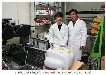
Professor Minyang Yang from the Department of Mechanical Engineering and his team developed a high-energy, flexible micro-supercapacitor in a simple and cost-effective way.
Compared to conventional micro-batteries, such as lithium-ion batteries, these new batteries, also called supercapacitors, are significantly faster to charge and semi-permanent.
Thin, flexible micro-supercapacitors can be a power source directly attached to wearable and flexible electronics.
However, fabrication of these micro-supercapacitors requires a complex patterning process, such as lithography techniques and vacuum evaporation. Hence, the process requires expensive instruments and toxic chemicals.
To simplify the fabrication of micro-supercapacitors in an eco-friendly manner, the team developed laser growth sintering technology. This technology manufactures superporous silver electrodes and applies them to the supercapacitors’ electrodes.
The team used a laser to form micro-patterns and generated nanoporous structures inside. This laser-induced growth sintering contributed to shortening the manufacturing process from ten steps to one.
Moreover, the team explored this unique laser growth sintering process –nucleation, growth, and sintering –by employing a particle-free, organometallic solution, which is not costly compared to typical laser-sintering methods for metallic nanoparticle solutions used in the printing of micro-electrodes.
Finally, unlike the typical supercapacitors comprised of a single substance, the team applied an asymmetric electrode configuration of nanoporous gold and manganese dioxide, which exhibits a highly-specific capacitance, to operate at a high voltage.
This method allows the team to develop energy storage with a high capacity. This developed micro-supercapacitor only requires four seconds to be charged and passed more than 5,000 durability tests.
Professor Yang said, “This research outcome can be used as energy storage installed in wearable and flexible electronic devices. Through this research, we are one step closer to realizing a complete version of flexible electronic devices by incorporating a power supply.”
This research, led by PhD candidate Jae Hak Lee, was selected as the cover of Journal of Materials Chemistry A on December 21, 2017.
Share on:


Suggested Items
Real Time with… IPC APEX EXPO 2024: Plasmatreat: Innovative Surface Preparation Solutions
04/25/2024 | Real Time with...IPC APEX EXPOIn this interview, Editor Nolan Johnson speaks with Hardev Grewal, CEO and president of Plasmatreat, a developer of atmospheric plasma solutions. Plasmatreat uses clean compressed air and electricity to create plasma, offering environmentally friendly methosd for surface preparation. Their technology measures plasma density for process optimization and can remove organic micro-contamination. Nolan and Hardev also discuss REDOX-Tool, a new technology for removing metal oxides.
KYZEN to Promote Pair of Stencil Cleaning Chemistries at SMTA Ciudad Jaurez Expo & Tech Forum
04/25/2024 | KYZEN'KYZEN, the global leader in innovative environmentally friendly cleaning chemistries, will exhibit at the SMTA Ciudad Juarez Expo & Tech Forum, scheduled to take place Thursday, May 9, 2024 at the Injectronic Convention Center in Ciudad Jaurez, Chihuahua, Mexico. During the event the KYZEN Clean Team will focus on understencil cleaning products KYZEN E5631J and CYBERSOLV C8882.
Cadence, TSMC Collaborate on Wide-Ranging Innovations to Transform System and Semiconductor Design
04/25/2024 | Cadence Design SystemsCadence Design Systems, Inc. and TSMC have extended their longstanding collaboration by announcing a broad range of innovative technology advancements to accelerate design, including developments ranging from 3D-IC and advanced process nodes to design IP and photonics.
Listen Up! The Intricacies of PCB Drilling Detailed in New Podcast Episode
04/25/2024 | I-Connect007In episode 5 of the podcast series, On the Line With: Designing for Reality, Nolan Johnson and Matt Stevenson continue down the manufacturing process, this time focusing on the post-lamination drilling process for PCBs. Matt and Nolan delve into the intricacies of the PCB drilling process, highlighting the importance of hole quality, drill parameters, and design optimization to ensure smooth manufacturing. The conversation covers topics such as drill bit sizes, aspect ratios, vias, challenges in drilling, and ways to enhance efficiency in the drilling department.
Designer’s Notebook: What Designers Need to Know About Manufacturing, Part 2
04/24/2024 | Vern Solberg -- Column: Designer's NotebookThe printed circuit board (PCB) is the primary base element for providing the interconnect platform for mounting and electrically joining electronic components. When assessing PCB design complexity, first consider the component area and board area ratio. If the surface area for the component interface is restricted, it may justify adopting multilayer or multilayer sequential buildup (SBU) PCB fabrication to enable a more efficient sub-surface circuit interconnect.