


 It’s Only Common Sense: OCCAM—the Time Is Now
 Marcy's Musings: The Growing Industry
 Dan’s Biz Bookshelf: Seeing the How
A Simpler Path
January 29, 2018 | A*STAREstimated reading time: 2 minutes
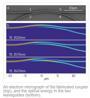
A core element of circuits handling optical signals can now be made smaller and simpler, and with functionality over a wider range of wavelengths, because of a mathematical model developed by A*STAR researchers. The new design methodology is expected to have widespread use in photonic integrated circuits and contribute to more compact photonic devices.
Optical signals, such as those transmitted over optical fiber, require photonic elements and circuits to be useful. One of the most important photonic functions is ‘coupling’, which allows the signal to be split into two different paths or used to drive other dependent circuits. Coupling, however, is generally only reliable over a narrow band of wavelengths, demanding a complicated design and fabrication process and bulkier circuits.
To overcome this obstacle to photonic circuit miniaturization, Jun Rong Ong and colleagues from the A*STAR Institute of High Performance Computing, in collaboration with researchers from the Singapore University of Technology and Design, went back to the drawing board to find a simpler approach to designing these critical coupling elements for broadband operation.
“Couplers are the basic building blocks of photonic circuits,” explains Ong. “However, it has been very difficult to try to make them compact, with low power loss and broadband operability, using standard processes.”
A coupler works by running a second optical path, known as a waveguide, alongside the signal path. The optical signal induces a secondary signal in the adjacent waveguide, passing with it some of the signal’s energy. However, the ratio of power splitting changes depending on the wavelength of the signal, so a broadband coupler that provides reliable performance over a wide range of useful wavelengths is something of a holy grail for photonics engineers.
“We distilled the key ingredient that makes a directional coupler a broadband splitter – a combination of straight and bent waveguides – and thoroughly explored and exploited it,” says Ong.
Ong’s team came up with a design methodology based on a mathematical ‘transfer matrix method’ to determine the coupler section lengths, radii, and waveguide cross-sections that would give the desired operation with low wavelength sensitivity. Using this approach, the team designed and fabricated a 50/50 power splitter with a wide bandwidth and length of just 20 micrometers.
“We were able to improve the broadband performance of the photonic power splitter through a simple modification of existing designs, and have achieved a balanced 50/50 output which is difficult by other designs,” Ong says.
Share on:


Suggested Items
Siemens’ Breakthrough Veloce CS Transforms Emulation and Prototyping with Three Novel Products
04/24/2024 | Siemens Digital Industries SoftwareSiemens Digital Industries Software launched the Veloce™ CS hardware-assisted verification and validation system. In a first for the EDA (Electronic Design Automation) industry, Veloce CS incorporates hardware emulation, enterprise prototyping and software prototyping and is built on two highly advanced integrated circuits (ICs) – Siemens’ new, purpose-built Crystal accelerator chip for emulation and the AMD Versal™ Premium VP1902 FPGA adaptive SoC (System-on-a-chip) for enterprise and software prototyping.
Elevating PCB Design Engineering With IPC Programs
04/24/2024 | Cory Blaylock, IPCIn a monumental stride for the electronics manufacturing industry, IPC has successfully championed the recognition of the PCB Design Engineer as an official occupation by the U.S. Department of Labor (DOL). This pivotal achievement not only underscores the critical role of PCB design engineers within the technology landscape, but also marks the beginning of a transformative journey toward nurturing a robust, skilled workforce ready to propel our industry into the future.
IPC Design Competition Champion Crowned at IPC APEX EXPO 2024
04/24/2024 | IPCAt IPC APEX EXPO 2024 in Anaheim, California, five competitors squared off to determine who was the best of the best at PCB design.
Altus Group Helps BitBox Unlock Productivity and Efficiency Gains with New Reflow Oven
04/22/2024 | Altus GroupAltus Group, a leading provider of capital equipment, has recently assisted BitBox, a UK-based electronics design, engineering and manufacturing company in upgrading its operations with the implementation of a new reflow oven from Heller Industries.
Real Time with... IPC APEX EXPO 2024: Exploring IPC's PCB Design Courses with Kris Moyer
04/18/2024 | Real Time with...IPC APEX EXPOGuest Editor Kelly Dack and IPC instructor Kris Moyer discuss IPC's PCB design training and education offerings. They delve into course topics such as design fundamentals, mil/aero, rigid-flex, RF design, and advanced design concepts. They also highlight material selection for high-speed design, thermal management, and dissipation techniques. The interview wraps up with details about how to access these courses online.