


 It’s Only Common Sense: OCCAM—the Time Is Now
 Marcy's Musings: The Growing Industry
 Dan’s Biz Bookshelf: Seeing the How
Optical Nanoscope Allows Imaging of Quantum Dots
February 1, 2018 | University of BaselEstimated reading time: 2 minutes
Physicists have developed a technique based on optical microscopy that can be used to create images of atoms on the nanoscale. In particular, the new method allows the imaging of quantum dots in a semiconductor chip. Together with colleagues from the University of Bochum, scientists from the University of Basel’s Department of Physics and the Swiss Nanoscience Institute reported the findings in the journal Nature Photonics.
Microscopes allow us to see structures that are otherwise invisible to the human eye. However, conventional optical microscopes cannot be used to image individual molecules and atoms, which measure just fractions of a nanometer across. This has to do with the wave nature of light and the associated laws of physics, which were formulated by the German physicist Ernst Abbe back in 1873.
According to these laws, a microscope’s maximum resolution is equal to half the wavelength of the light used. For example, if you use green light with a wavelength of 500 nanometers, an optical microscope can, at best, distinguish objects at a distance of 250 nanometers.
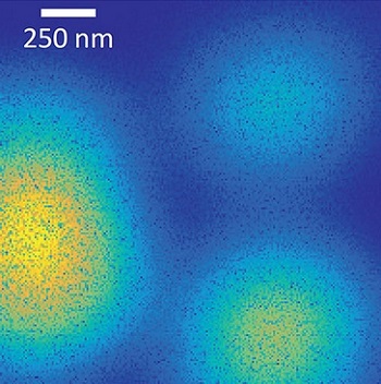
Image of quantum dots in a semiconductor: whereas the image taken with a normal microscope is blurry (left), the new method (right) clearly shows four quantum dots (bright yellow spots). (Image: University of Basel, Department of Physics)
Switched on and off
In recent years, however, scientists have managed to get around this resolution limit and generate images of structures measuring just a few nanometers across. To do so, they used lasers of various wavelengths to trigger fluorescence in molecules in part of the substance while suppressing it in the surrounding areas. This allows them to image structures such as dye molecules, which are just a few nanometers in size. The development of this method (Stimulated Emission Depletion, STED) was honored with the Nobel Prize in Chemistry 2014.
For all objects with two energy levels
Timo Kaldewey, from Professor Richard Warburton’s team at the University of Basel’s Department of Physics and Swiss Nanoscience Institute, has now worked with colleagues at Ruhr-University Bochum (Germany) to develop a similar technique that allows the imaging of nanoscale objects, particularly a quantum mechanical two-level system.
The physicists studied what are known as quantum dots, artificial atoms in a semiconductor, which the new method was able to image as bright spots. The scientists excited the atoms with a pulsed laser, which changes its color during each pulse. As a result, the atom’s fluorescence is switched on and off.
Whereas the STED method only works by occupying at least four different energy levels in response to the laser excitation, the new method from Basel also works with atoms that have just two energy states. Two-state systems of this kind constitute important model systems for quantum mechanics.
Unlike STED microscopy, the new method also releases no heat. “This is a huge advantage, as any heat released can destroy the molecules you’re examining,” explains Richard Warburton. “Our nanoscope is suitable for all objects with two energy levels, such as real atoms, cold molecules, quantum dots, or color centers.”
The project received funding from, among other sources, the National Center of Competence in Research “Quantum Science and Technology” (NCCR QSIT), the Swiss National Science Foundation, and the European Union under the FP7 program.
Share on:


Suggested Items
Inkjet Solder Mask ‘Has Arrived’
04/10/2024 | Pete Starkey, I-Connect007I was delighted to be invited to attend an interactive webinar entitled “Solder Mask Coating Made Easy with Additive Manufacturing,” hosted by SUSS MicroTec Netherlands in Eindhoven. The webinar was introduced and moderated by André Bodegom, managing director at Adeon Technologies, and the speakers were Mariana Van Dam, senior product manager PCB imaging solutions at AGFA in Belgium; Ashley Steers, sales manager at Electra Polymers in the UK; and Dr. Luca Gautero, product manager at SUSS MicroTec Netherlands.
NetVia Group Acquires Direct Imaging from Mivatek
04/09/2024 | Miva TechnologiesMiva Technologies is pleased to announce NetVia Group, Irving, TX has acquired a new Miva 2400NG Dual Tray Direct Imaging System with 30-micron capabilities for inner, outer and soldermask imaging.
Teledyne to Acquire Adimec
02/13/2024 | TeledyneTeledyne Technologies Incorporated announced that it has entered into an agreement to acquire Adimec Holding B.V. and its subsidiaries.
Real Time with... productronica 2023: MivaTek Global Advances Technology With High-res Imaging System
12/08/2023 | Real Time with...productronicaMivaTek's Brendan Hogan talks about how the company employs Digitally Adaptive Rasterization Technology (DART) in their high-res imaging equipment. He also shares how the blurred line between semiconductors and microelectronics is driving broader application of the imaging process.
Keysight Enables Validation of Arbe 4D Imaging Radar Chipset
11/30/2023 | Keysight Technologies, Inc.Keysight Technologies, Inc. announces that Arbe has selected the E8719A Radar Target Solution (RTS) to test the Arbe 4D imaging radar chipset for automotive applications.