


 It’s Only Common Sense: OCCAM—the Time Is Now
 Marcy's Musings: The Growing Industry
 Dan’s Biz Bookshelf: Seeing the How
Study Reveals Secrets of ‘Fluid-like’ Heat Flow in Solid Semiconductor at Nanoscale
February 1, 2018 | Purdue UniversityEstimated reading time: 3 minutes
Researchers are applying the same “hydrodynamic transport model” used to study flow in fluids to explain heat transport in a solid semiconductor, with potential implications for the design of high-speed transistors and lasers.
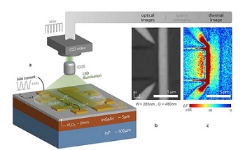
Image caption: Purdue University researchers have visualized temperature changes produced by ultra-small heat sources, gold strips formed on top of the semiconductor indium gallium arsenide. The work has potential implications for the design of high-speed transistors and lasers. This image (a) depicts the device structure and experimental setup, an optical image (b) of the fabricated device and (c) an experimental thermal image. (Purdue University image/Amirkoushyar Ziabari, Bjorn Vermeersch)
Thermal imaging of tiny nanoscale semiconductor heat sources revealed details about vortices of heat-carrying objects called phonons.
The new findings have potentially important implications for “thermal crosstalk,” in which multiple heat sources next to each other impact the overall temperature of the system, hindering performance. The researchers used a technique called full-field thermoreflectance thermal imaging to directly visualize temperature changes produced by ultra-small heat sources, gold strips formed on top of the semiconductor indium gallium arsenide.
The research concerns the crucial role of phonons, quantum-mechanical objects, or “quasiparticles,” that describe how vibrations travel through a material's crystal structure. The phonons are said to be “heat carriers” in solid materials.
“This is the first time such hydrodynamic effects are indirectly observed for heat propagation in a solid,” said Ali Shakouri, Purdue University's Mary Jo and Robert L. Kirk Director of the Birck Nanotechnology Center and a professor of electrical and computer engineering. “While structures called vortices are common in fluid flows such as water or air, this is the first time we’ve seen that they can be present inside solids for phonon flow in the typical semiconductor indium gallium arsenide, which is used in high-speed transistors and lasers.”
“The observed thermal crosstalk reduction has important implications in the design of nanoscale electronic and optoelectronic devices,” said Purdue postdoctoral research associate Amirkoushyar Ziabari, the paper’s lead author. “As the size of electronic and optoelectronic devices are getting smaller, there are more and more devices being packed into a smaller area, so the thermal crosstalk between these devices becomes important. Knowing the accurate thermal behavior in the neighborhood and a few microns from heat sources would help design better state-of-the-art devices in terms of performance, speed, thermal reliability, and so on.”
The researchers found that the reduced thermal crosstalk is caused by vortices generated near the edge of the heat sources.
“This is similar to the vortices that are observed at the edge of an obstacle placed inside of a current of air or water, such as behind an airplane wing,” Shakouri said.
The governing law of heat conduction, known as the Fourier Law or the heat-diffusion equation, does not accurately predict thermal transport for devices on the nanoscale. Because the Fourier diffusion equation doesn't explain the heat transport at those scales, this transport regime is called non-diffusive.
“As the size of electronic and optoelectronic devices are getting smaller, it is important to consider this non-diffusive behavior for design and optimization of such small devices,” Ziabari said. “These new measurements show that at nanoscales, heat propagation has interesting ‘fluid-like’ behavior.”
Conventional methods do not account for vortices of heat transport found at the nanoscale.
“Vorticity only becomes important when the characteristic source dimension is comparable to the hydrodynamic length scale of about 150 nanometers,” he said.
The Fourier theory substantially overestimates the experimentally observed temperature a short distance away from the heater lines.
“The surprising effect was that the temperature decays much faster than what Fourier theory predicted,” Shakouri said. “Within a distance of 1 or 2 microns of a small heat source - a line about 100 nanometers wide - temperature could be one-third to one-fourth what Fourier theory predicts.”
The thermoreflectance thermal imaging approach allows researchers to create maps of temperature rise at far higher resolution than otherwise possible using light in the visible range.
The work was performed by researchers at the Birck Nanotechnology Center in Purdue’s Discovery Park, Purdue’s School of Electrical and Computer Engineering, Universitat Autónoma de Barcelona, Commissariat à l’Énergie Atomique in Grenoble, France, and the Department of Mechanical and Materials Engineering at the University of Cincinnati. All co-authors are listed in the abstract.
The research was partially funded by the European Commission and the Spanish Ministry of Economy and Competitiveness.
Share on:


Suggested Items
Cadence, TSMC Collaborate on Wide-Ranging Innovations to Transform System and Semiconductor Design
04/25/2024 | Cadence Design SystemsCadence Design Systems, Inc. and TSMC have extended their longstanding collaboration by announcing a broad range of innovative technology advancements to accelerate design, including developments ranging from 3D-IC and advanced process nodes to design IP and photonics.
Ansys, TSMC Enable a Multiphysics Platform for Optics and Photonics, Addressing Needs of AI, HPC Silicon Systems
04/25/2024 | PRNewswireAnsys announced a collaboration with TSMC on multiphysics software for TSMC's Compact Universal Photonic Engines (COUPE). COUPE is a cutting-edge Silicon Photonics (SiPh) integration system and Co-Packaged Optics platform that mitigates coupling loss while significantly accelerating chip-to-chip and machine-to-machine communication.
Siemens’ Breakthrough Veloce CS Transforms Emulation and Prototyping with Three Novel Products
04/24/2024 | Siemens Digital Industries SoftwareSiemens Digital Industries Software launched the Veloce™ CS hardware-assisted verification and validation system. In a first for the EDA (Electronic Design Automation) industry, Veloce CS incorporates hardware emulation, enterprise prototyping and software prototyping and is built on two highly advanced integrated circuits (ICs) – Siemens’ new, purpose-built Crystal accelerator chip for emulation and the AMD Versal™ Premium VP1902 FPGA adaptive SoC (System-on-a-chip) for enterprise and software prototyping.
Elevating PCB Design Engineering With IPC Programs
04/24/2024 | Cory Blaylock, IPCIn a monumental stride for the electronics manufacturing industry, IPC has successfully championed the recognition of the PCB Design Engineer as an official occupation by the U.S. Department of Labor (DOL). This pivotal achievement not only underscores the critical role of PCB design engineers within the technology landscape, but also marks the beginning of a transformative journey toward nurturing a robust, skilled workforce ready to propel our industry into the future.
IPC Design Competition Champion Crowned at IPC APEX EXPO 2024
04/24/2024 | IPCAt IPC APEX EXPO 2024 in Anaheim, California, five competitors squared off to determine who was the best of the best at PCB design.