


 Marcy's Musings: The Growing Industry
 It’s Only Common Sense: Here’s What To Do After IPC APEX EXPO 2024
 Dan’s Biz Bookshelf: Seeing the How
Experiments Confirm First Chiral Phonon that Could Enable Exotic Forms of Electronics
February 2, 2018 | Lawrence Berkeley National LaboratoryEstimated reading time: 5 minutes
A research team from the Department of Energy’s Lawrence Berkeley National Laboratory (Berkeley Lab) has found the first evidence that a shaking motion in the structure of an atomically thin (2-D) material possesses a naturally occurring circular rotation.
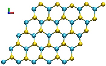
The atomic motion in a 2-D material, tungsten disulfide, is shown in this animation. In this phonon mode (known as longitudinal optical mode or LO), the selenium atoms (yellow) rotate clockwise while the tungsten atoms (blue) are still. (Credit: Hanyu Zhu, et al.)
This rotation could become the building block for a new form of information technology, and for the design of molecular-scale rotors to drive microscopic motors and machines.
The monolayer material, tungsten diselenide (WSe2), is already well-known for its unusual ability to sustain special electronic properties that are far more fleeting in other materials.
It is considered a promising candidate for a sought-after form of data storage known as valleytronics, for example, in which the momentum and wavelike motion of electrons in a material can be sorted into opposite “valleys” in a material’s electronic structure, with each of these valleys representing the ones and zeroes in conventional binary data.
Modern electronics typically rely on manipulations of the charge of electrons to carry and store information, though as electronics are increasingly miniaturized they are more subject to problems associated with heat buildup and electric leaks.
The latest study, published online this week in the journal Science, provides a possible path to overcome these issues. It reports that some of the material’s phonons, a term describing collective vibrations in atomic crystals, are naturally rotating in a certain direction.
This property is known as chirality – similar to a person’s handedness where the left and right hand are a mirror image of each other but not identical. Controlling the direction of this rotation would provide a stable mechanism to carry and store information.
“Phonons in solids are usually regarded as the collective linear motion of atoms,” said Xiang Zhang, the corresponding author of the study and senior scientist of the Materials Science Division at Lawrence Berkeley National Laboratory and professor at UC Berkeley. “Our experiment discovered a new type of so-called chiral phonons where atoms move in circles in an atomic monolayer crystal of tungsten diselenide.”
Hanyu Zhu, the lead author of the study and a postdoctoral researcher at Zhang’s group, said, “One of the biggest advantage of chiral phonon is that the rotation is locked with the particle’s momentum and not easily disturbed.”
In the phonon mode studied, the selenium atoms appear to collectively rotate in a clockwise direction, while the tungsten atoms showed no motion. Researchers prepared a “sandwich” with four sheets of centimeter-sized monolayer WSe2 samples placed between thin sapphire crystals. They synced ultrafast lasers to record the time-dependent motions.
The two laser sources converged on a spot on the samples measuring just 70 millionths of a meter in diameter. One of the lasers was precisely switched between two different tuning modes to sense the difference of left and right chiral phonon activity.
Image - This diagram shows atomic motion in separate phonon modes. At left ("LO" represents a longitudinal optical mode), selenium atoms exhibit a clockwise rotation while tungsten atoms stand still. At right ("LA" represents a longitudinal acoustic mode), tungsten atoms exhibit a clockwise rotation while selenium atoms rotate in a counterclockwise direction. (Credit: Hanyu Zhu, et al.)
This diagram maps out atomic motion in separate phonon modes. At left (“LO” represents a longitudinal optical mode), selenium atoms exhibit a clockwise rotation while tungsten atoms stand still. At right (“LA” represents a longitudinal acoustic mode), tungsten atoms exhibit a clockwise rotation while selenium atoms rotate in a counterclockwise direction. (Credit: Hanyu Zhu, et al.)
A so-called pump laser produced visible, red-light pulses that excited the samples, and a probe laser produced mid-infrared pulses that followed the first pump pulse within one trillionth of a second. About one mid-infrared photon in every 100 million is absorbed by WSe2 and converted to a chiral phonon.
The researchers then captured the high-energy luminescence from the sample, a signature of this rare absorption event. Through this technique, known as transient infrared spectroscopy, researchers not only confirmed the existence of a chiral phonon but also accurately obtained its rotational frequency.
So far, the process only produces a small number of chiral phonons. A next step in the research will be to generate larger numbers of rotating phonons, and to learn whether vigorous agitations in the crystal can be used to flip the spin of electrons or to significantly alter the valley properties of the material. Spin is an inherent property of an electron that can be thought of as its compass needle – if it could be flipped to point either north or south it could be used to convey information in a new form of electronics called spintronics.
“The potential phonon-based control of electrons and spins for device applications is very exciting and within reach,” Zhu said. “We already proved that phonons are capable of switching the electronic valley. In addition, this work allows the possibility of using the rotating atoms as little magnets to guide the spin orientation.”
The chiral properties found in the study likely exist across a wide range of 2-D materials based on a similar patterning in their atomic structure, Zhu also noted, adding that the study could guide theoretical investigations of electron-phonon interactions and the design of materials to enhance phonon-based effects.
“The same principle works in all 2-D periodic structures with three-fold symmetry and inversion asymmetry” Zhu said. “The same principle covers a huge family of natural materials, and there are almost infinite possibilities for creating rotors at the molecular scale.”
Researchers at UC Berkeley, King Abdullah University of Science and Technology in Saudi Arabia, and Nanjing Normal University in China also participated in the study. This work was primarily supported by the U.S. Department of Energy’s Office of Science.
About Lawrence Berkeley National Laboratory
Lawrence Berkeley National Laboratory addresses the world’s most urgent scientific challenges by advancing sustainable energy, protecting human health, creating new materials, and revealing the origin and fate of the universe. Founded in 1931, Berkeley Lab’s scientific expertise has been recognized with 13 Nobel Prizes. The University of California manages Berkeley Lab for the U.S. Department of Energy’s Office of Science.
Share on:


Suggested Items
Groundbreaking Ceremony Marks the Beginning of a New Era for Newccess Industrial; The Construction of the MINGXIN Building
04/12/2024 | Newccess IndustrialOn a clear and sunny day in March, the groundbreaking ceremony for the MINGXIN Building took place in Shenzhen, China. This moment marked the official commencement of construction for a project that will reshape the semiconductor materials industry.
The Need for a Holistic Global Sustainability Standard
04/10/2024 | Michael Ford, Aegis SoftwareNo one can deny that the resources of our fragile planet are finite. The environment seems like a third party, subject to constant degradation. We’re acutely aware of the effects of pollution on our climate, and despite our “throw-away” culture, recycling and recovery of materials has remained relatively expensive, even as we use more energy just to survive.
iNEMI Publishes Four Roadmap Topics
04/04/2024 | iNEMIThe International Electronics Manufacturing Initiative (iNEMI) announces the availability of the first roadmap topics in the new iNEMI Roadmap format. Printed circuit boards, sustainable electronics, smart manufacturing, and mmWave materials and test are now available online.
Insulectro’s 'Storekeepers' Extend Their Welcome to Technology Village at IPC APEX EXPO
04/03/2024 | InsulectroInsulectro, the largest distributor of materials for use in the manufacture of PCBs and printed electronics, welcomes attendees to its TECHNOLOGY VILLAGE during this year’s IPC APEX EXPO at the Anaheim Convention Center, April 9-11, 2024.
Checking In With ICAPE Group
04/03/2024 | Nolan Johnson, I-Connect007ICAPE Group’s field application engineer Erik Pederson drills down on sustainability, supply chain resiliency, and what value engineering really looks like in this exclusive interview. Founded in 1999, European-based ICAPE Group provides 21 million printed circuit boards and over six million technical parts to manufacturers every month. With 30 PCB manufacturing partners globally and 50 partners providing a wide array of technical parts, ICAPE Group has operations in China, Taiwan, Thailand, South Korea, Vietnam, South Africa, Europe, Mexico, and the United States. The company also focuses on the value proposition for its customers.